メインコンテンツにスキップ
Moov logo

Moov Icon
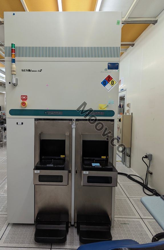
APPLIED MATERIALS (AMAT) SEMVISION G2
    説明
    Applied Materials SEMVision STAR Defect Analysis, Scanning Electron Microscope
    構成
    Inspection LD: 2ea, AsystInspection SEM
    OEMモデルの説明
    The AMAT SEMVision G2 is a high-throughput, fully automatic Defect Analysis system developed by Applied Materials (AMAT). It is designed to be seamlessly integrated into production lines, allowing customers to analyze defects with exceptional productivity. The system is capable of detecting and analyzing defects as small as 50nm, providing crucial insights into the quality and performance of semiconductor devices during manufacturing.
    ドキュメント

    ドキュメントなし

    APPLIED MATERIALS (AMAT)

    SEMVISION G2

    verified-listing-icon

    検証済み

    カテゴリ

    Defect Inspection
    最終検証: 7日前
    主なアイテムの詳細

    状態:

    Used


    稼働ステータス:

    Installed / Running


    製品ID:

    93121


    ウェーハサイズ:

    不明


    ヴィンテージ:

    2002

    Have Additional Questions?
    Logistics Support
    Available
    Money Back Guarantee
    Available
    Transaction Insured by Moov
    Available
    Refurbishment Services
    Available
    同様のリスト
    すべて表示

    同様のリストが見つかりません

    APPLIED MATERIALS (AMAT)

    SEMVISION G2

    verified-listing-icon

    検証済み

    カテゴリ

    Defect Inspection
    最終検証: 7日前
    listing-photo-c89cd99bdfdf4144bfa1a5df91ac5861-https://media-moov-co.s3.us-west-1.amazonaws.com/user_media/listingPhoto/54780/c89cd99bdfdf4144bfa1a5df91ac5861/4b124db5d65b4ddf8fa8d9f1f9f98eea_ce1c2ccb0b464f2ca67b7a0bb0b4de961201a_mw.jpeg
    listing-photo-c89cd99bdfdf4144bfa1a5df91ac5861-https://media-moov-co.s3.us-west-1.amazonaws.com/user_media/listingPhoto/54780/c89cd99bdfdf4144bfa1a5df91ac5861/d0c8cad12fca4d51ac7b1b22a1f60a54_f7f4e352053a4d8fb2c44e0937cffbc51201a_mw.jpeg
    listing-photo-c89cd99bdfdf4144bfa1a5df91ac5861-https://media-moov-co.s3.us-west-1.amazonaws.com/user_media/listingPhoto/54780/c89cd99bdfdf4144bfa1a5df91ac5861/865a97938552461d89c1c8d6169ed976_ca745668795c43d8af2f8241f15e11ad_mw.jpeg
    listing-photo-c89cd99bdfdf4144bfa1a5df91ac5861-https://media-moov-co.s3.us-west-1.amazonaws.com/user_media/listingPhoto/54780/c89cd99bdfdf4144bfa1a5df91ac5861/5618de6998ce4b67be6b275746e17105_eb0dbbb20e4446faa45288cde9beb4771201a_mw.jpeg
    listing-photo-c89cd99bdfdf4144bfa1a5df91ac5861-https://media-moov-co.s3.us-west-1.amazonaws.com/user_media/listingPhoto/54780/c89cd99bdfdf4144bfa1a5df91ac5861/f95295823ca14766bc8a747bbc716db6_aaec410f9eda474fa765478eebf144b21201a_mw.jpeg
    listing-photo-c89cd99bdfdf4144bfa1a5df91ac5861-https://media-moov-co.s3.us-west-1.amazonaws.com/user_media/listingPhoto/54780/c89cd99bdfdf4144bfa1a5df91ac5861/6ae7a303e2f34887ad41622ab8182848_903427f94c9e4a7cb11358ee62b56c041201a_mw.jpeg
    listing-photo-c89cd99bdfdf4144bfa1a5df91ac5861-https://media-moov-co.s3.us-west-1.amazonaws.com/user_media/listingPhoto/54780/c89cd99bdfdf4144bfa1a5df91ac5861/40bb58210e694f349931186ac6c3798d_0ac015029dd9453e92215734690effaf1201a_mw.jpeg
    listing-photo-c89cd99bdfdf4144bfa1a5df91ac5861-https://media-moov-co.s3.us-west-1.amazonaws.com/user_media/listingPhoto/54780/c89cd99bdfdf4144bfa1a5df91ac5861/4ea4bc25cd674183b88db98e50203c26_2260dcb43f3f4661bbe3d704818ffedc1201a_mw.jpeg
    listing-photo-c89cd99bdfdf4144bfa1a5df91ac5861-https://media-moov-co.s3.us-west-1.amazonaws.com/user_media/listingPhoto/54780/c89cd99bdfdf4144bfa1a5df91ac5861/3de50ef8267d490f8c93ea8ecfb85c00_852b31c16726400794086408f22ae2131201a_mw.jpeg
    主なアイテムの詳細

    状態:

    Used


    稼働ステータス:

    Installed / Running


    製品ID:

    93121


    ウェーハサイズ:

    不明


    ヴィンテージ:

    2002


    Logistics Support
    Available
    Money Back Guarantee
    Available
    Transaction Insured by Moov
    Available
    Refurbishment Services
    Available
    説明
    Applied Materials SEMVision STAR Defect Analysis, Scanning Electron Microscope
    構成
    Inspection LD: 2ea, AsystInspection SEM
    OEMモデルの説明
    The AMAT SEMVision G2 is a high-throughput, fully automatic Defect Analysis system developed by Applied Materials (AMAT). It is designed to be seamlessly integrated into production lines, allowing customers to analyze defects with exceptional productivity. The system is capable of detecting and analyzing defects as small as 50nm, providing crucial insights into the quality and performance of semiconductor devices during manufacturing.
    ドキュメント

    ドキュメントなし

    同様のリスト
    すべて表示

    同様のリストが見つかりません