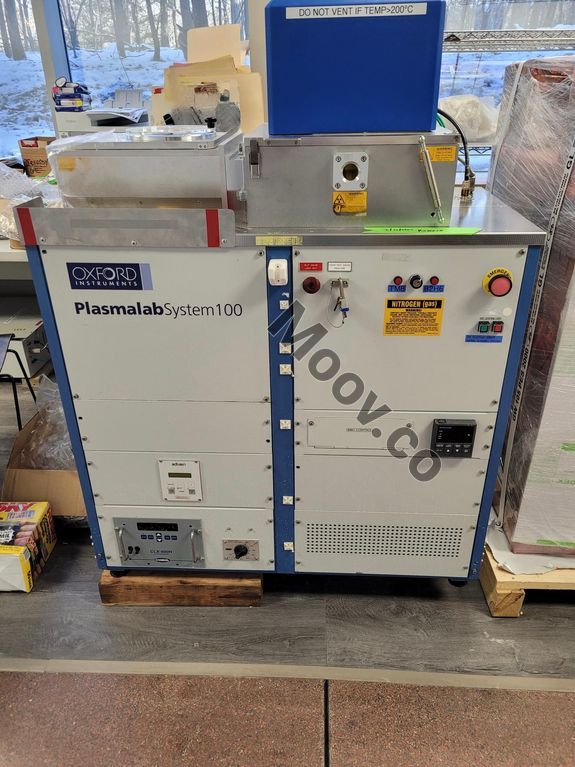
説明
-Recently de-installed, but not operational (there is a wafer transport issue) -Full gas cabinet included構成
Oxford Plasmalab 100 PECVD: -Configured for 200mm wafers, with Al carrier for multiple substrate sizes, down to small pieces -Used for deposition of SiO2 and Si3N4 -Optional low-frequency power supply (configured with dual-frequency RF) -Heated stage; Routinely ran at 370 degrees -MFCs for 7 gases - Ar, CF4/O2, SiH4, N2O, CH4, PH3/TMP, and B2H6/TMBOEMモデルの説明
The Oxford Plasmalab 100 is an inductively coupled plasma (ICP) etcher that is designed for multipurpose use. It is based on fluorocarbon and is capable of anisotropically etching silicon, silicon oxide, and other dielectric materials. The tool is equipped with a temperature-controlled electrode, which allows users to tailor their etch feature profiles. The manual load system can accommodate substrates of various sizes, ranging from 200mm diameter wafers down to small piecesドキュメント
ドキュメントなし
カテゴリ
PECVD
最終検証: 30日以上前
主なアイテムの詳細
状態:
Used
稼働ステータス:
不明
製品ID:
106186
ウェーハサイズ:
4"/100mm, 5"/125mm, 6"/150mm, 8"/200mm
ヴィンテージ:
2001
Logistics Support
Available
Transaction Insured by Moov
Available
Refurbishment Services
Available
同様のリスト
すべて表示OXFORD
PLASMALAB 100 PECVD
カテゴリ
PECVD
最終検証: 30日以上前
主なアイテムの詳細
状態:
Used
稼働ステータス:
不明
製品ID:
106186
ウェーハサイズ:
4"/100mm, 5"/125mm, 6"/150mm, 8"/200mm
ヴィンテージ:
2001
Logistics Support
Available
Transaction Insured by Moov
Available
Refurbishment Services
Available
説明
-Recently de-installed, but not operational (there is a wafer transport issue) -Full gas cabinet included構成
Oxford Plasmalab 100 PECVD: -Configured for 200mm wafers, with Al carrier for multiple substrate sizes, down to small pieces -Used for deposition of SiO2 and Si3N4 -Optional low-frequency power supply (configured with dual-frequency RF) -Heated stage; Routinely ran at 370 degrees -MFCs for 7 gases - Ar, CF4/O2, SiH4, N2O, CH4, PH3/TMP, and B2H6/TMBOEMモデルの説明
The Oxford Plasmalab 100 is an inductively coupled plasma (ICP) etcher that is designed for multipurpose use. It is based on fluorocarbon and is capable of anisotropically etching silicon, silicon oxide, and other dielectric materials. The tool is equipped with a temperature-controlled electrode, which allows users to tailor their etch feature profiles. The manual load system can accommodate substrates of various sizes, ranging from 200mm diameter wafers down to small piecesドキュメント
ドキュメントなし