

説明
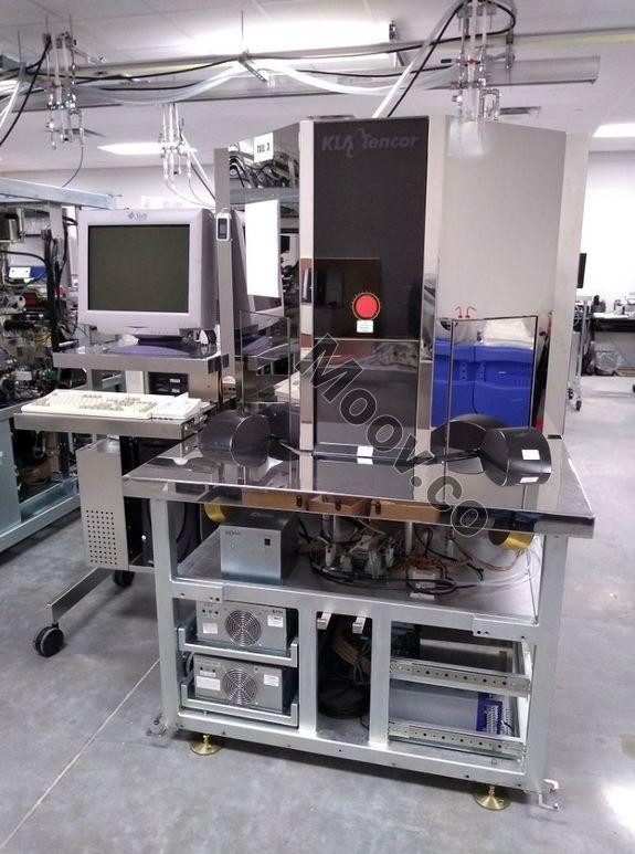
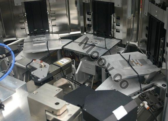
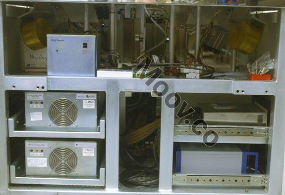
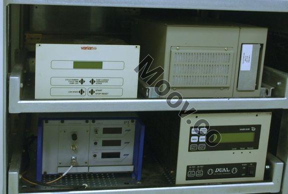
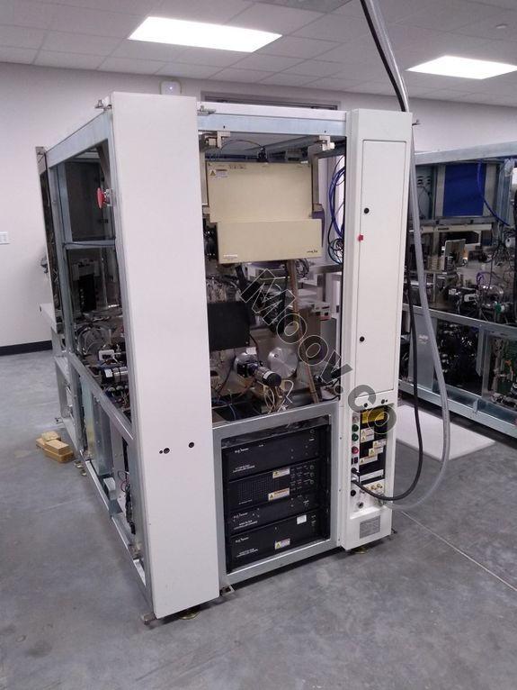
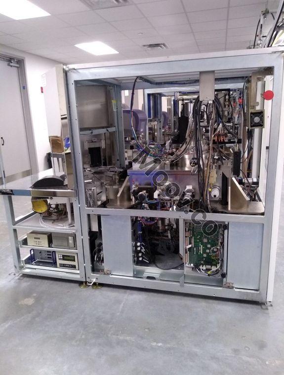
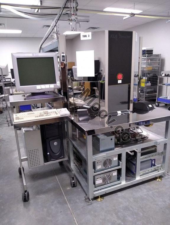
CD SEM構成
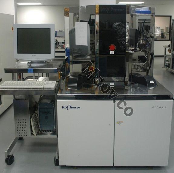
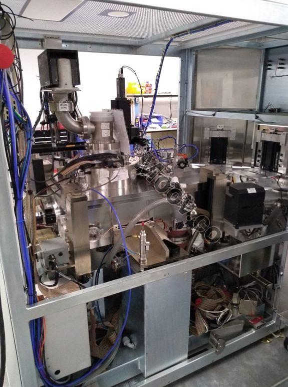
NT Platform System Computer Dell Precision Work Station (Dual Core Processor) Raid Array (2 drive) OS – Windows NT 4.0 Main System Application – 6.1.SR2+ 3 Cassette Stations – Wafer 4” 5” 6” 8” Capable PRI Robot (with Class 1 wafer scanner) and Prealigner Electron Column – E Column Electron Source – Refurbished Scintillator Detector – New Energy Filter – Refurbished Wein Filter Apertures (2 each) – New Quick Pump (Optional)OEMモデルの説明
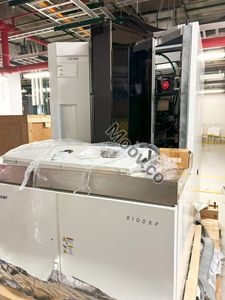
The KLA-Tencor 8100XP CD SEM is a state-of-the-art scanning electron microscope used in semiconductor manufacturing. It enables precise and fast measurements of critical dimensions (CD) in small device geometries. The CD SEM has advanced capabilities for imaging and measuring high aspect ratio features, ensuring optimum device performance. It offers productivity-enhancing features such as high throughput, networking, offline recipe setup, and full system automation.ドキュメント
ドキュメントなし
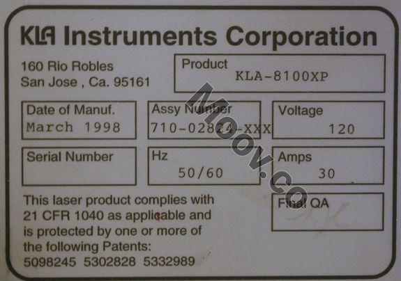
KLA
8100XP

検証済み
カテゴリ
CD-SEM
主なアイテムの詳細
状態:
Used
稼働ステータス:
不明
製品ID:
49393
ウェーハサイズ:
4"/100mm, 5"/125mm, 6"/150mm, 8"/200mm
ヴィンテージ:
1998
Have Additional Questions?
Logistics Support
Available
Money Back Guarantee
Available
Transaction Insured by Moov
Available
Refurbishment Services
Available

KLA
8100XP
検証済み
カテゴリ
CD-SEM
最終検証: 60日以上前

主なアイテムの詳細
状態:
Used
稼働ステータス:
不明
製品ID:
49393
ウェーハサイズ:
4"/100mm, 5"/125mm, 6"/150mm, 8"/200mm
ヴィンテージ:
1998
Logistics Support
Available
Money Back Guarantee
Available
Transaction Insured by Moov
Available
Refurbishment Services
Available
説明
CD SEM構成
NT Platform System Computer Dell Precision Work Station (Dual Core Processor) Raid Array (2 drive) OS – Windows NT 4.0 Main System Application – 6.1.SR2+ 3 Cassette Stations – Wafer 4” 5” 6” 8” Capable PRI Robot (with Class 1 wafer scanner) and Prealigner Electron Column – E Column Electron Source – Refurbished Scintillator Detector – New Energy Filter – Refurbished Wein Filter Apertures (2 each) – New Quick Pump (Optional)OEMモデルの説明
The KLA-Tencor 8100XP CD SEM is a state-of-the-art scanning electron microscope used in semiconductor manufacturing. It enables precise and fast measurements of critical dimensions (CD) in small device geometries. The CD SEM has advanced capabilities for imaging and measuring high aspect ratio features, ensuring optimum device performance. It offers productivity-enhancing features such as high throughput, networking, offline recipe setup, and full system automation.ドキュメント
ドキュメントなし