





説明
説明なし構成
構成なしOEMモデルの説明
The Applied SEMVision G7 system offers greater imaging variety and advances in automatic defect classification (ADC) based on expanded machine learning capabilities. Besides the imaging capabilities of the previous SEMVision generation, the new system offers unique imaging of the wafer-edge bevel and apex where undetected defects can reduce device yield. To achieve robust review of unpatterned wafers, an enhanced light source and collection mechanism combined with improved noise suppression enable optical detection of defects as small as 18nm.ドキュメント
ドキュメントなし

カテゴリ
Defect Inspection
最終検証: 30日以上前
主なアイテムの詳細
状態:
Used
稼働ステータス:
不明
製品ID:
150294
ウェーハサイズ:
不明
ヴィンテージ:
不明
Logistics Support
Available
Transaction Insured by Moov
Available
Refurbishment Services
Available
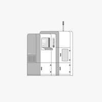
APPLIED MATERIALS (AMAT)
SEMVISION G7
カテゴリ
Defect Inspection
最終検証: 30日以上前


主なアイテムの詳細
状態:
Used
稼働ステータス:
不明
製品ID:
150294
ウェーハサイズ:
不明
ヴィンテージ:
不明
Logistics Support
Available
Transaction Insured by Moov
Available
Refurbishment Services
Available
説明
説明なし構成
構成なしOEMモデルの説明
The Applied SEMVision G7 system offers greater imaging variety and advances in automatic defect classification (ADC) based on expanded machine learning capabilities. Besides the imaging capabilities of the previous SEMVision generation, the new system offers unique imaging of the wafer-edge bevel and apex where undetected defects can reduce device yield. To achieve robust review of unpatterned wafers, an enhanced light source and collection mechanism combined with improved noise suppression enable optical detection of defects as small as 18nm.ドキュメント
ドキュメントなし