


説明
説明なし構成
構成なしOEMモデルの説明
Applied UVision® 3 system, the industry’s highest productivity DUV1 Brightfield wafer inspection tool with the critical-defect detection sensitivity required for 45 nanometer (nm) FEOL2 and immersion lithography. Delivering significant advancements to Applied’s breakthrough UVision technology, this next-generation system triples the number of laser beams scanning the wafer to provide 40% faster throughput than any competitive system. Two new imaging modes extend sensitivity to 20nm, and a new flexible automatic defect classification engine enables quick access to defects of interest and faster yield learning. imaging modes in the illumination and collection path which address the contrast versatility required for periphery areas; innovative algorithms of high defect accuracy and stitch-to-stitch detection enable enhanced sensitivity on edge of array and on high-end devices; dual screen configuration with High Resolution Review, which minimizes SEM review time; and new automatic classification capabilities provide quick access to defect-of-interest to reduce yield learning cycle. Additionally, UVision 3’s proprietary ActiveScan technique dynamically compensates for process and color variations within and across wafers.ドキュメント
ドキュメントなし

カテゴリ
Defect Inspection
最終検証: 60日以上前
主なアイテムの詳細
状態:
Used
稼働ステータス:
不明
製品ID:
29600
ウェーハサイズ:
不明
ヴィンテージ:
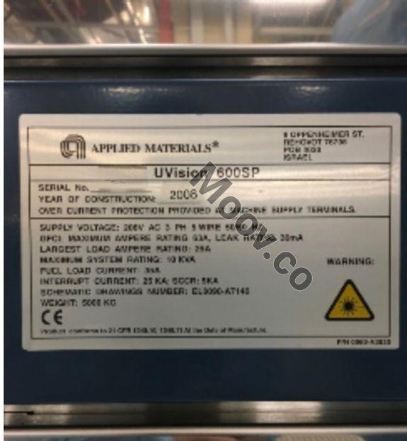
2008
Logistics Support
Available
Transaction Insured by Moov
Available
Refurbishment Services
Available
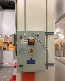
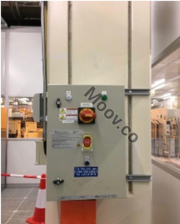
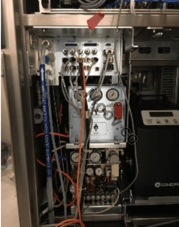
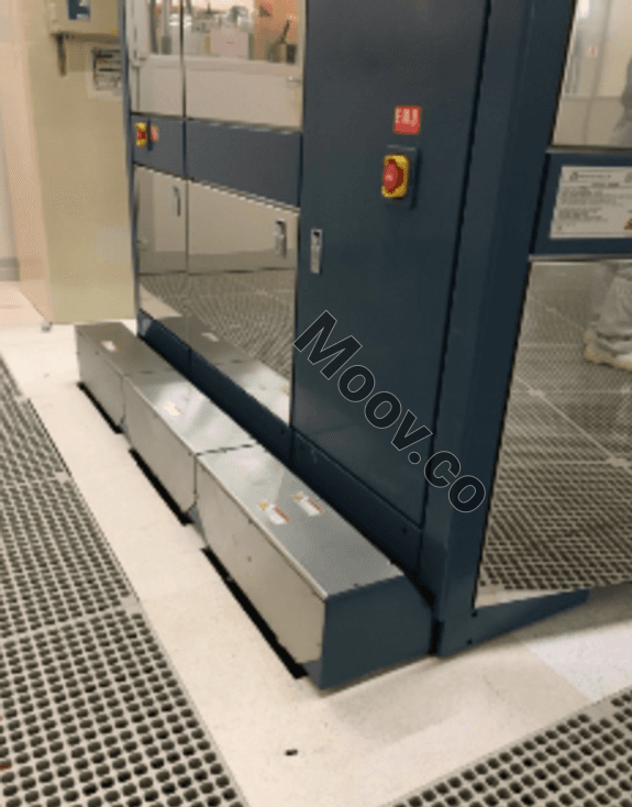
APPLIED MATERIALS (AMAT)
UVISION 3
カテゴリ
Defect Inspection
最終検証: 60日以上前

主なアイテムの詳細
状態:
Used
稼働ステータス:
不明
製品ID:
29600
ウェーハサイズ:
不明
ヴィンテージ:
2008
Logistics Support
Available
Transaction Insured by Moov
Available
Refurbishment Services
Available
説明
説明なし構成
構成なしOEMモデルの説明
Applied UVision® 3 system, the industry’s highest productivity DUV1 Brightfield wafer inspection tool with the critical-defect detection sensitivity required for 45 nanometer (nm) FEOL2 and immersion lithography. Delivering significant advancements to Applied’s breakthrough UVision technology, this next-generation system triples the number of laser beams scanning the wafer to provide 40% faster throughput than any competitive system. Two new imaging modes extend sensitivity to 20nm, and a new flexible automatic defect classification engine enables quick access to defects of interest and faster yield learning. imaging modes in the illumination and collection path which address the contrast versatility required for periphery areas; innovative algorithms of high defect accuracy and stitch-to-stitch detection enable enhanced sensitivity on edge of array and on high-end devices; dual screen configuration with High Resolution Review, which minimizes SEM review time; and new automatic classification capabilities provide quick access to defect-of-interest to reduce yield learning cycle. Additionally, UVision 3’s proprietary ActiveScan technique dynamically compensates for process and color variations within and across wafers.ドキュメント
ドキュメントなし