


説明
説明なし構成
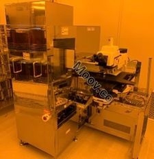
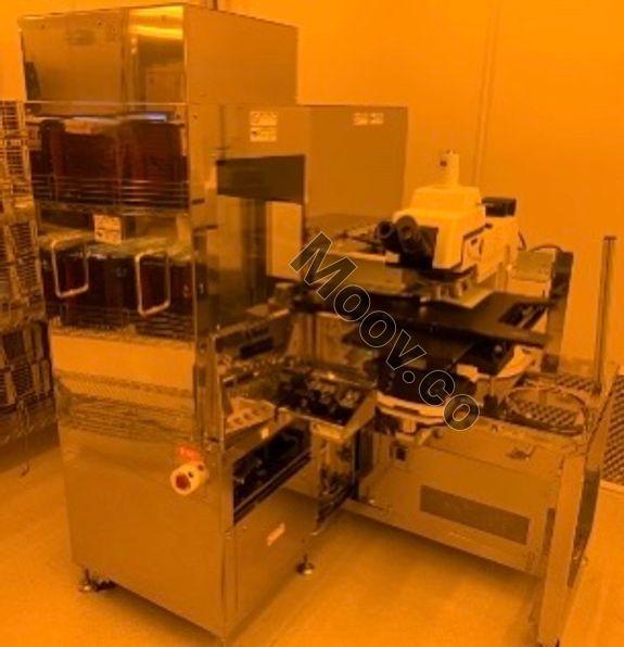
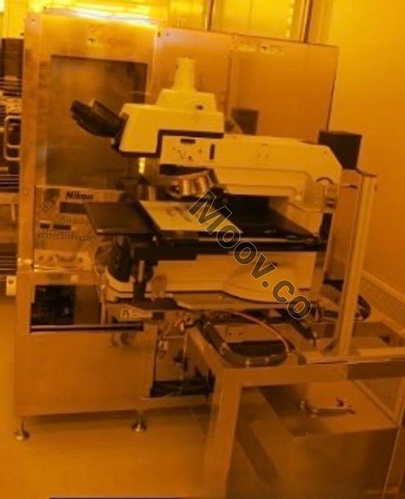
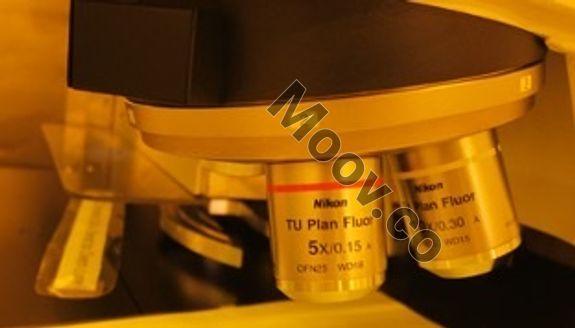
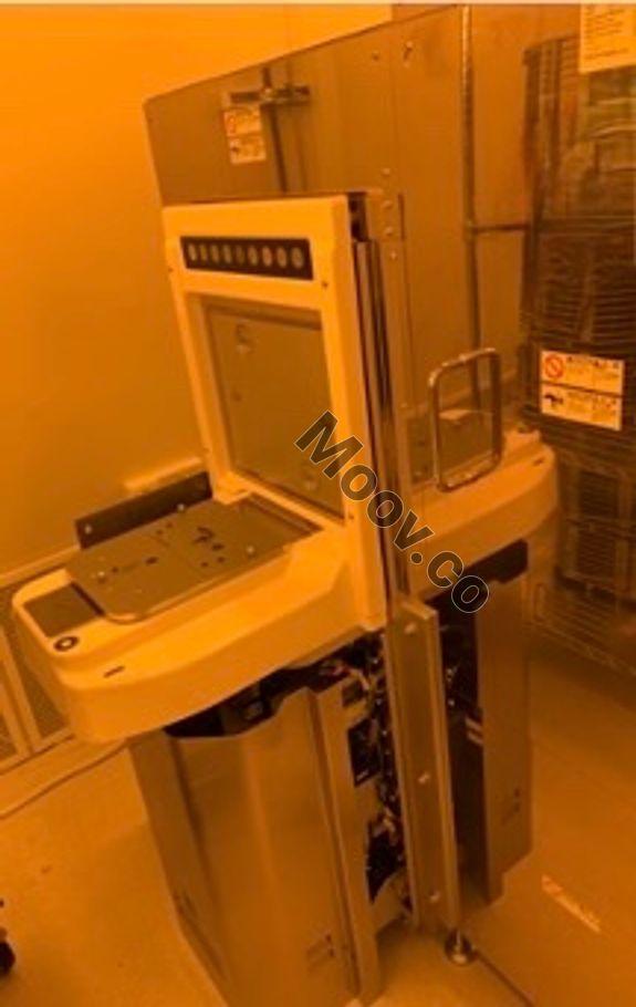
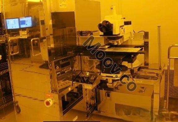
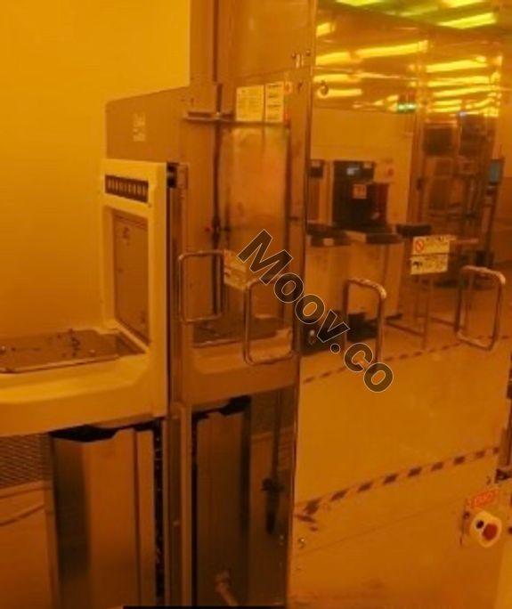
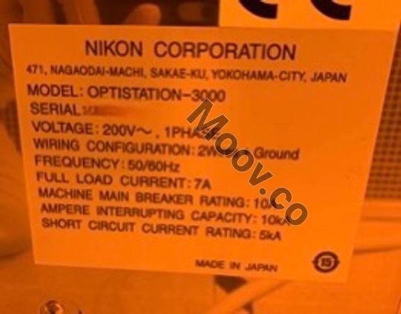
Semi-Auto (Auto wafer handler),12" only. Specifications Wafer size: 300 mm (SEMI / M1.15 /t = 750 -20 um), Standard cassette types: FOUP, FOSB, and FFO Micro inspection: Surface, backside, edge, and macro image capture functions Wafer alignment: Non-contact alignment Wafer transfer system: High-speed, multi-axis robot Microscope: Nikon L300 300mm wafer inspection microscope (brightfield/darkfield and DIC observation) Expandability: 200mm wafer transfer, deformed wafer transfer, and thin wafer transfer Power usage: Power supply: 200 VAC -10%, max. 10A, 50/60 Hz Vacuum: -66.7 kPa/-30 NI/min Stage: Manual vacuum contact stage with 360° rotation System reliability: MTBF 1500 hours, Up time > 95%OEMモデルの説明
OPTISTATION-3000 wafer inspection system.ドキュメント

カテゴリ
Defect Inspection
最終検証: 60日以上前
主なアイテムの詳細
状態:
Used
稼働ステータス:
不明
製品ID:
66601
ウェーハサイズ:
不明
ヴィンテージ:
不明
Logistics Support
Available
Transaction Insured by Moov
Available
Refurbishment Services
Available

NIKON
OPTISTATION-3000
カテゴリ
Defect Inspection
最終検証: 60日以上前

主なアイテムの詳細
状態:
Used
稼働ステータス:
不明
製品ID:
66601
ウェーハサイズ:
不明
ヴィンテージ:
不明
Logistics Support
Available
Transaction Insured by Moov
Available
Refurbishment Services
Available