


説明
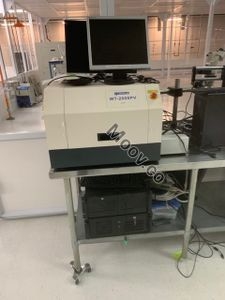
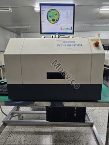
Semilab WT-2000PVN( μ-PCD) Carrier life time measurement *. Fully refurbished. *. Installed in Clean-room. *. Can demonstrate any time.構成
■ System Configuration . WT2000PV main unit with scanning capability . Sample stage (Max wafer size 200mm) . Dual PC : DOS PC & Window PC . μ-PCD head for lifetime measurements . Application S/W : Wintau 32 ( Windows PC ) . Vacuum pump . Utility : - Power : 220V or 115V, 50/60Hz - Vacuum : 1/4" 0.2 ~0.5 bar ■ Hardware Function Capability . μ-PCD measurement (904 nm Laser) . Laser Power Feedback . Automatic Head Height . Capacitive Sensor . Head Temperature Sensor . Others ■ Application . Monitoring defects and contamination ( bulk and surface region of Si wafer) ■ Measurement . Carrier Lifetime Measurement (μ-PCD), Laser wavelength : 904nm . High resolution mapping and discrete point measurementsOEMモデルの説明
The Semilab WT-2000PVN is a compact measurement system that can perform a range of measurements on photovoltaic (PV) cells, wafers, and blocks. The system comes with overhead functions and can be customized to meet your specific measurement needs by choosing from the available options. The WT-2000PVN is capable of measuring both blocks and ingots, as well as wafers and cells. When measuring wafers and cells, maps are typically produced, while line scans are often used for blocks or ingots to save time. However, the WT-2000PVN can do both. Many PV cell manufacturers use the WT-2000PVN for engineering development, characterization, production batch testing, and troubleshooting production issues. The system can be integrated with various measurement techniques, including µ-PCD/carrier lifetime, SHR/sheet resistance, LBIC/photovoltaic response, quantum efficiency, diffusion length, and eddy current/non-contact resistivity mapping.ドキュメント
ドキュメントなし


SEMILAB
WT-2000PV
カテゴリ
Defect Inspection
最終検証: 60日以上前


主なアイテムの詳細
状態:
Used
稼働ステータス:
不明
製品ID:
66028
ウェーハサイズ:
8"/200mm
ヴィンテージ:
2009
Logistics Support
Available
Transaction Insured by Moov
Available
Refurbishment Services
Available
説明
Semilab WT-2000PVN( μ-PCD) Carrier life time measurement *. Fully refurbished. *. Installed in Clean-room. *. Can demonstrate any time.構成
■ System Configuration . WT2000PV main unit with scanning capability . Sample stage (Max wafer size 200mm) . Dual PC : DOS PC & Window PC . μ-PCD head for lifetime measurements . Application S/W : Wintau 32 ( Windows PC ) . Vacuum pump . Utility : - Power : 220V or 115V, 50/60Hz - Vacuum : 1/4" 0.2 ~0.5 bar ■ Hardware Function Capability . μ-PCD measurement (904 nm Laser) . Laser Power Feedback . Automatic Head Height . Capacitive Sensor . Head Temperature Sensor . Others ■ Application . Monitoring defects and contamination ( bulk and surface region of Si wafer) ■ Measurement . Carrier Lifetime Measurement (μ-PCD), Laser wavelength : 904nm . High resolution mapping and discrete point measurementsOEMモデルの説明
The Semilab WT-2000PVN is a compact measurement system that can perform a range of measurements on photovoltaic (PV) cells, wafers, and blocks. The system comes with overhead functions and can be customized to meet your specific measurement needs by choosing from the available options. The WT-2000PVN is capable of measuring both blocks and ingots, as well as wafers and cells. When measuring wafers and cells, maps are typically produced, while line scans are often used for blocks or ingots to save time. However, the WT-2000PVN can do both. Many PV cell manufacturers use the WT-2000PVN for engineering development, characterization, production batch testing, and troubleshooting production issues. The system can be integrated with various measurement techniques, including µ-PCD/carrier lifetime, SHR/sheet resistance, LBIC/photovoltaic response, quantum efficiency, diffusion length, and eddy current/non-contact resistivity mapping.ドキュメント
ドキュメントなし