AutoWafer
概要(Overview)
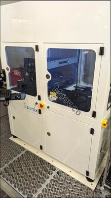
AutoWafer is an ultrasonic wafer scanner for nondestructive testing (NDT) of wafers in development and production environments, providing high-resolution identification of bond defects in wafer applications such as MEMS, CMOS, memory, TSV and LED. Robotic cassette handling and sorting of approved and failed wafers helps speed production, while our advanced transducers and auto-analysis tools make it quick and easy to identify even the smallest, most subtle defects. -The ideal automatic ultrasonic testing system for detecting wafer-to-wafer bonding defects -A fully automated, production-ready wafer scanner for MEMS, CMOS, BSI sensors, memory, TSV, LED and other applications employing wafers 200mm and smaller -Provides wafer map with die-level pass/fail indicators (optional) -Provides analysis (optional) -200mm SECS/GEM -TSV entrenched metrology
現在の掲載品
1
サービス
検査、保証、鑑定、ロジスティクス