


説明
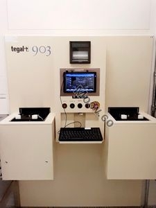
Gas Lines: 4 The Tegal 903e plasma dry etch semiconductor equipment were made by Tegal Corporation and represents the Industry Standard in single-wafer Dry Etch of Polysilicon, Nitride, Silicon Oxide and the mainstay of the highly successful plasma etch system. The Tegal 903e plasma dry etch semiconductor equipment are used by the semiconductor industry for integrated circuit fabrication. Tegal 903e plasma etcher plasma etch semiconductor equipment are used in one part of the sequence of manufacturing steps that transfer a pattern formed from a layer of photosensitive material, the photoresist, to a layer that makes up a permanent part of the finished device. Wafers in the Tegal 903e plasma dry etch semiconductor equipment are transported to a Reaction Chamber. A gas mixture is introduced into the Reaction Chamber, and the gas mixture is caused to become reactive by the application of radio frequency (RF) electromagnetic radiation. The reactive mixture, or plasma, etches away material that is not covered by the masking photoresist. The etch process is terminated at an appropriate time, the wafer is unloaded from the Reaction Chamber, and a new wafer is introduced. The cycle repeats. The Tegal 903e plasma dry etch semiconductor equipment Plasma/RlE etchers have been configured to take advantage of the characteristics of plasmas for etching various films. Each of the models in the 90Xe family have been optimized for specific etches of specific films. All models have the common ability to implement multi-step etch recipes using multiple process gases. An optical monitoring system provides a means for determining etch completion so that the etch process may be terminated.構成
構成なしOEMモデルの説明
The Tegal 903e is an inline RIE/plasma production etcher configured for six-inch wafers. It is a single-wafer, cassette-to-cassette driven tool with easy-to-use menu control and a 13.56 MHz RF Generator. The input gases are controlled by MFC, with up to 4 MFCs in the system. This tool implements multi-step etch recipes using multiple process gases and has been optimized for specific etches of specific films. Gases available in this configuration are N2, O2, SF6, CHF3, and He. The Tegal 903e plasma dry etch equipment is used by the semiconductor industry for integrated circuit fabrication. It is an industry standard in single-wafer dry etch of silicon nitride, polysilicon, amorphous silicon, and silicon oxide. Wafers are transported to a reaction chamber utilizing a non-friction spatula wafer transport mechanism. A gas mixture is introduced into the Reaction Chamber and becomes reactive by the application of radio frequency (RF) electromagnetic radiation. The reactive mixture, or plasma, etches away material that is not covered by the masking photoresist. The etch process is terminated by time (a parameter specified in the recipe), the wafer is unloaded from the reaction chamber, and a new wafer is introduced repeating the cycle until all wafers have been processed.ドキュメント
ドキュメントなし

同様のリスト
すべて表示


TEGAL
903E
カテゴリ
Dry / Plasma Etch
最終検証: 60日以上前


主なアイテムの詳細
状態:
Refurbished
稼働ステータス:
不明
製品ID:
138622
ウェーハサイズ:
3"/75mm, 4"/100mm, 5"/125mm, 6"/150mm
ヴィンテージ:
不明
Logistics Support
Available
Transaction Insured by Moov
Available
Refurbishment Services
Available
説明
Gas Lines: 4 The Tegal 903e plasma dry etch semiconductor equipment were made by Tegal Corporation and represents the Industry Standard in single-wafer Dry Etch of Polysilicon, Nitride, Silicon Oxide and the mainstay of the highly successful plasma etch system. The Tegal 903e plasma dry etch semiconductor equipment are used by the semiconductor industry for integrated circuit fabrication. Tegal 903e plasma etcher plasma etch semiconductor equipment are used in one part of the sequence of manufacturing steps that transfer a pattern formed from a layer of photosensitive material, the photoresist, to a layer that makes up a permanent part of the finished device. Wafers in the Tegal 903e plasma dry etch semiconductor equipment are transported to a Reaction Chamber. A gas mixture is introduced into the Reaction Chamber, and the gas mixture is caused to become reactive by the application of radio frequency (RF) electromagnetic radiation. The reactive mixture, or plasma, etches away material that is not covered by the masking photoresist. The etch process is terminated at an appropriate time, the wafer is unloaded from the Reaction Chamber, and a new wafer is introduced. The cycle repeats. The Tegal 903e plasma dry etch semiconductor equipment Plasma/RlE etchers have been configured to take advantage of the characteristics of plasmas for etching various films. Each of the models in the 90Xe family have been optimized for specific etches of specific films. All models have the common ability to implement multi-step etch recipes using multiple process gases. An optical monitoring system provides a means for determining etch completion so that the etch process may be terminated.構成
構成なしOEMモデルの説明
The Tegal 903e is an inline RIE/plasma production etcher configured for six-inch wafers. It is a single-wafer, cassette-to-cassette driven tool with easy-to-use menu control and a 13.56 MHz RF Generator. The input gases are controlled by MFC, with up to 4 MFCs in the system. This tool implements multi-step etch recipes using multiple process gases and has been optimized for specific etches of specific films. Gases available in this configuration are N2, O2, SF6, CHF3, and He. The Tegal 903e plasma dry etch equipment is used by the semiconductor industry for integrated circuit fabrication. It is an industry standard in single-wafer dry etch of silicon nitride, polysilicon, amorphous silicon, and silicon oxide. Wafers are transported to a reaction chamber utilizing a non-friction spatula wafer transport mechanism. A gas mixture is introduced into the Reaction Chamber and becomes reactive by the application of radio frequency (RF) electromagnetic radiation. The reactive mixture, or plasma, etches away material that is not covered by the masking photoresist. The etch process is terminated by time (a parameter specified in the recipe), the wafer is unloaded from the reaction chamber, and a new wafer is introduced repeating the cycle until all wafers have been processed.ドキュメント
ドキュメントなし