


説明
説明なし構成
IBA_HiCurOEMモデルの説明
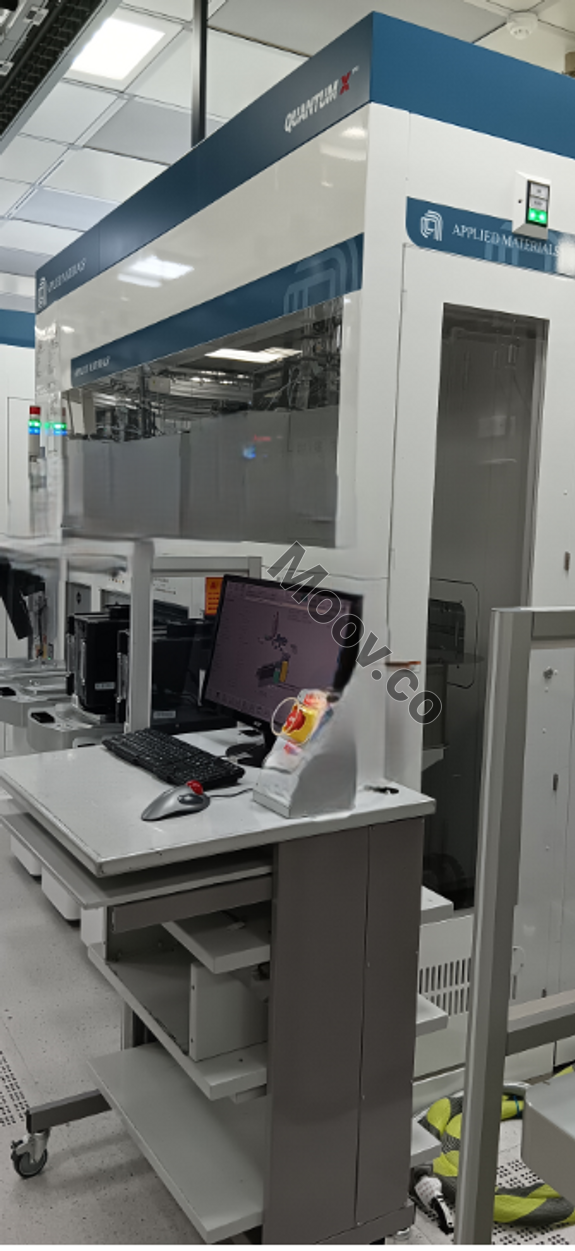
The Applied Quantum X Implant system, along with Applied's other technologies, meets the strict requirements for 65nm transistors. It offers high throughput at low energies, uniformity across all points and wafers, and precise motion control to prevent particle damage. The system is extendible to new applications for advanced logic and memory devices. Quantum X redefines fab productivity for high current ion implantation by providing single-wafer precision, ultra-low defect levels, and high throughput. Its innovative technology enables extendibility to high tilt implant and other new applications at 65nm and beyond. It features high throughput at low energies (200eV - 80keV) with all points, all wafers uniformity and two-dimensional parallel scanning with StepScan™ fixed beam technology for single wafer processing and up to 60° tilt angleドキュメント
ドキュメントなし

カテゴリ
High Current
最終検証: 22日前
主なアイテムの詳細
状態:
Used
稼働ステータス:
不明
製品ID:
144796
ウェーハサイズ:
12"/300mm
ヴィンテージ:
2006
Logistics Support
Available
Transaction Insured by Moov
Available
Refurbishment Services
Available


APPLIED MATERIALS (AMAT)
QUANTUM X
カテゴリ
High Current
最終検証: 22日前


主なアイテムの詳細
状態:
Used
稼働ステータス:
不明
製品ID:
144796
ウェーハサイズ:
12"/300mm
ヴィンテージ:
2006
Logistics Support
Available
Transaction Insured by Moov
Available
Refurbishment Services
Available
説明
説明なし構成
IBA_HiCurOEMモデルの説明
The Applied Quantum X Implant system, along with Applied's other technologies, meets the strict requirements for 65nm transistors. It offers high throughput at low energies, uniformity across all points and wafers, and precise motion control to prevent particle damage. The system is extendible to new applications for advanced logic and memory devices. Quantum X redefines fab productivity for high current ion implantation by providing single-wafer precision, ultra-low defect levels, and high throughput. Its innovative technology enables extendibility to high tilt implant and other new applications at 65nm and beyond. It features high throughput at low energies (200eV - 80keV) with all points, all wafers uniformity and two-dimensional parallel scanning with StepScan™ fixed beam technology for single wafer processing and up to 60° tilt angleドキュメント
ドキュメントなし