


説明
The Heidelberg Instruments DWL-66 is a versatile laser-based system designed for advanced mask production and wafer patterning. Utilizing a HeCd laser, it achieves fine resolution down to 800 nm through meticulous alignment and control of the laser optics. Fully operational and still installed.構成
442 nm wavelength, 300 mW, HeCd laser (replaced in 2014, has around 4400 hours of usage) 4 mm write head 20 mm write head Flowbox Greyscale exposure Upgraded computer to Windows 7 in 2019 Metrology and Alignment PackageOEMモデルの説明
The DWL 66 is a precise, maskless laser lithography system for various applications like maskless lithography, photomask making, and direct writing. It supports gray-scale exposures on flat, photosensitive-coated materials. Key features include a minimum feature size of 0.6 microns, substrate size up to 200 x 200 mm, and over 1.0M dpi resolution using a 20-nanometer address grid.ドキュメント
ドキュメントなし

カテゴリ
Lithography
最終検証: 60日以上前
主なアイテムの詳細
状態:
Used
稼働ステータス:
Installed / Running
製品ID:
115928
ウェーハサイズ:
不明
Laser:
442
ヴィンテージ:
2002
Logistics Support
Available
Transaction Insured by Moov
Available
Refurbishment Services
Available

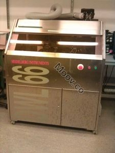
HEIDELBERG INSTRUMENTS
DWL 66
カテゴリ
Lithography
最終検証: 60日以上前


主なアイテムの詳細
状態:
Used
稼働ステータス:
Installed / Running
製品ID:
115928
ウェーハサイズ:
不明
Laser:
442
ヴィンテージ:
2002
Logistics Support
Available
Transaction Insured by Moov
Available
Refurbishment Services
Available
説明
The Heidelberg Instruments DWL-66 is a versatile laser-based system designed for advanced mask production and wafer patterning. Utilizing a HeCd laser, it achieves fine resolution down to 800 nm through meticulous alignment and control of the laser optics. Fully operational and still installed.構成
442 nm wavelength, 300 mW, HeCd laser (replaced in 2014, has around 4400 hours of usage) 4 mm write head 20 mm write head Flowbox Greyscale exposure Upgraded computer to Windows 7 in 2019 Metrology and Alignment PackageOEMモデルの説明
The DWL 66 is a precise, maskless laser lithography system for various applications like maskless lithography, photomask making, and direct writing. It supports gray-scale exposures on flat, photosensitive-coated materials. Key features include a minimum feature size of 0.6 microns, substrate size up to 200 x 200 mm, and over 1.0M dpi resolution using a 20-nanometer address grid.ドキュメント
ドキュメントなし