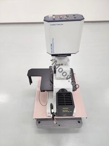
We value your privacy
We and our selected partners use cookies to enhance your browsing experience, serve personalized content, and analyze our traffic. By clicking "Accept All", you consent to our use of cookies. 続きを読む
"Semiconductor wafer inspection microscope (up to 200 mm) enabling fast, accurate inspection via motorized aperture stop interlocked with objective lens. Ergonomic design delivers operator comfort. SEMI S2/S8 compliance ensures safety and reliability."
7
検査、保証、鑑定、ロジスティクス