


説明
説明なし構成
構成なしOEMモデルの説明
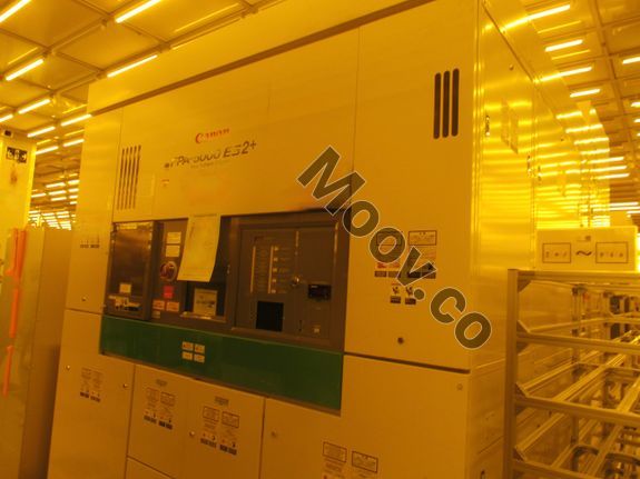
The FPA-5000ES2+ is a high-throughput 248-nanometer scanner for 0.15-micron ICs, introduced by Canon U.S.A. Inc.'s Semiconductor Equipment Division. It uses a 2-kilohertz, krypton-fluoride (KrF) excimer laser to expose 125 eight-inch wafers an hour and is aimed at a growing need for highly productive scanners with both 200- and 300-mm wafer capability. It has been designed to handle both 0.18- and 0.15-micron design rules, and allows field conversion from 200-mm to 300-mm wafer format within a day. It offers a 25% increase in throughput compared with its predecessor, the FPA-5000ES2.ドキュメント
ドキュメントなし

カテゴリ
Steppers & Scanners
最終検証: 60日以上前
主なアイテムの詳細
状態:
Used
稼働ステータス:
不明
製品ID:
110081
ウェーハサイズ:
不明
ヴィンテージ:
2000
Logistics Support
Available
Transaction Insured by Moov
Available
Refurbishment Services
Available

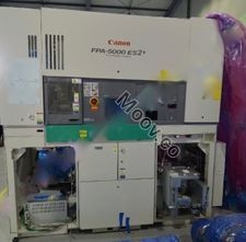

CANON
FPA-5000ES2+
カテゴリ
Steppers & Scanners
最終検証: 60日以上前


主なアイテムの詳細
状態:
Used
稼働ステータス:
不明
製品ID:
110081
ウェーハサイズ:
不明
ヴィンテージ:
2000
Logistics Support
Available
Transaction Insured by Moov
Available
Refurbishment Services
Available
説明
説明なし構成
構成なしOEMモデルの説明
The FPA-5000ES2+ is a high-throughput 248-nanometer scanner for 0.15-micron ICs, introduced by Canon U.S.A. Inc.'s Semiconductor Equipment Division. It uses a 2-kilohertz, krypton-fluoride (KrF) excimer laser to expose 125 eight-inch wafers an hour and is aimed at a growing need for highly productive scanners with both 200- and 300-mm wafer capability. It has been designed to handle both 0.18- and 0.15-micron design rules, and allows field conversion from 200-mm to 300-mm wafer format within a day. It offers a 25% increase in throughput compared with its predecessor, the FPA-5000ES2.ドキュメント
ドキュメントなし