


説明
Waferbonder構成
構成なしOEMモデルの説明
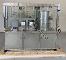
Automated production bonding system for a wide range of fusion/molecular wafer bonding applications SOI wafers are a promising new basic material for the microelectronics industry to produce faster and higher-performance microelectronic devices. Wafer bonding, as one key enabling technology for the SOI wafer fabrication process, achieves high-quality single-crystal silicon films on insulating substrates. With the EVG850 SOI production bonding system, all essential steps for SOI bonding – from cleaning and alignment to pre-bonding and IR-inspection – are combined. Thus, the EVG850 assures a high-yield production process for void-free SOI wafers up to 300 mm sizes. Being the only production system built to operate in high-throughput, high-yield environments, the EVG850 has been established as the industry standard in the SOI wafer market.ドキュメント
ドキュメントなし

カテゴリ
Wafer Bonders
最終検証: 60日以上前
主なアイテムの詳細
状態:
Used
稼働ステータス:
不明
製品ID:
41200
ウェーハサイズ:
8"/200mm
ヴィンテージ:
2012
Logistics Support
Available
Transaction Insured by Moov
Available
Refurbishment Services
Available
同様のリスト
すべて表示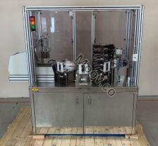


EVGroup (EVG)
EVG850
カテゴリ
Wafer Bonders
最終検証: 60日以上前


主なアイテムの詳細
状態:
Used
稼働ステータス:
不明
製品ID:
41200
ウェーハサイズ:
8"/200mm
ヴィンテージ:
2012
Logistics Support
Available
Transaction Insured by Moov
Available
Refurbishment Services
Available
説明
Waferbonder構成
構成なしOEMモデルの説明
Automated production bonding system for a wide range of fusion/molecular wafer bonding applications SOI wafers are a promising new basic material for the microelectronics industry to produce faster and higher-performance microelectronic devices. Wafer bonding, as one key enabling technology for the SOI wafer fabrication process, achieves high-quality single-crystal silicon films on insulating substrates. With the EVG850 SOI production bonding system, all essential steps for SOI bonding – from cleaning and alignment to pre-bonding and IR-inspection – are combined. Thus, the EVG850 assures a high-yield production process for void-free SOI wafers up to 300 mm sizes. Being the only production system built to operate in high-throughput, high-yield environments, the EVG850 has been established as the industry standard in the SOI wafer market.ドキュメント
ドキュメントなし