


説明
Bright Field構成
Bright FieldOEMモデルの説明
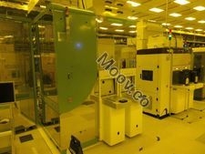
The Applied UVision 5 wafer inspection system detects yield-limiting defects in the critical patterning layers of 22nm and below logic and memory devices. Applied also offers the Applied DFinder system, the first darkfield wafer inspection system to use DUV laser scanning to detect particles as small as 40nm in interconnect layers. The UVision® 5 system isa member of the UVision wafer inspection product family, supporting the same proprietary core technology of deep ultraviolet (DUV) laser illumination, with simultaneous dual channel [brightfield (BF) reflected light and grayfield (GF) scattered light] collection optics. The system exhibits new defect inspection capabilities on advanced patterning layers in both FEOL and BEOL applications for 2xnm production and beyond, addressing such technologies as ArF immersion lithography, double and quad patterning, and extreme ultraviolet layers. The UVision 5 system’s dramatically increased light density enables detection of 1xnm killer defects - some never captured before - resulting in a twofold improvement in killer defect capture rates. This, in turn, results in a more accurate and comprehensive defect Pareto that significantly improves statistical process control in the wafer fab. The platform’s unique GF detection architecture now captures more light to enable detection of defects in the range of 1xnm (approximately the width of up to five DNA strands). New imaging modes improve detection sensitivity to further increase UVision technology leadership in GF scanning. Novel image processing algorithms reduce wafer noise by up to 50% in various types of memory structures, contributing to a higher capture rate, especially on BEOL layers.ドキュメント
ドキュメントなし

カテゴリ
Defect Inspection
最終検証: 60日以上前
主なアイテムの詳細
状態:
Used
稼働ステータス:
不明
製品ID:
40359
ウェーハサイズ:
12"/300mm
ヴィンテージ:
2011
Logistics Support
Available
Transaction Insured by Moov
Available
Refurbishment Services
Available
同様のリスト
すべて表示
APPLIED MATERIALS (AMAT)
UVISION 5
カテゴリ
Defect Inspection
最終検証: 60日以上前


主なアイテムの詳細
状態:
Used
稼働ステータス:
不明
製品ID:
40359
ウェーハサイズ:
12"/300mm
ヴィンテージ:
2011
Logistics Support
Available
Transaction Insured by Moov
Available
Refurbishment Services
Available
説明
Bright Field構成
Bright FieldOEMモデルの説明
The Applied UVision 5 wafer inspection system detects yield-limiting defects in the critical patterning layers of 22nm and below logic and memory devices. Applied also offers the Applied DFinder system, the first darkfield wafer inspection system to use DUV laser scanning to detect particles as small as 40nm in interconnect layers. The UVision® 5 system isa member of the UVision wafer inspection product family, supporting the same proprietary core technology of deep ultraviolet (DUV) laser illumination, with simultaneous dual channel [brightfield (BF) reflected light and grayfield (GF) scattered light] collection optics. The system exhibits new defect inspection capabilities on advanced patterning layers in both FEOL and BEOL applications for 2xnm production and beyond, addressing such technologies as ArF immersion lithography, double and quad patterning, and extreme ultraviolet layers. The UVision 5 system’s dramatically increased light density enables detection of 1xnm killer defects - some never captured before - resulting in a twofold improvement in killer defect capture rates. This, in turn, results in a more accurate and comprehensive defect Pareto that significantly improves statistical process control in the wafer fab. The platform’s unique GF detection architecture now captures more light to enable detection of defects in the range of 1xnm (approximately the width of up to five DNA strands). New imaging modes improve detection sensitivity to further increase UVision technology leadership in GF scanning. Novel image processing algorithms reduce wafer noise by up to 50% in various types of memory structures, contributing to a higher capture rate, especially on BEOL layers.ドキュメント
ドキュメントなし