


説明
Operational upon removal from the fab. Skidded, vapor barrier bagged, wrapped. Not crated. Complete systems, with no missing parts.構成
構成なしOEMモデルの説明
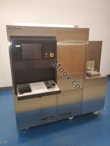
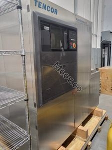
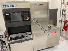
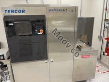
The AIT In-line Defect Inspection System is a high-throughput system that uses proprietary double-darkfield (DDF) laser scanning technology to detect defects, microscratches, and particulate contamination on wafers. It can inspect up to 30 wafers per hour at maximum sensitivity and has a low cost-per-inspection, making it economically feasible to perform in-line process monitoring at more process levels. The system achieves exceptional defect sensitivity through innovations such as a reduced laser spot size and a unique double-darkfield laser scattering design.ドキュメント
ドキュメントなし

同様のリスト
すべて表示


KLA
AIT I
カテゴリ
Defect Inspection
最終検証: 60日以上前


主なアイテムの詳細
状態:
Used
稼働ステータス:
不明
製品ID:
131730
ウェーハサイズ:
不明
ヴィンテージ:
不明
Logistics Support
Available
Transaction Insured by Moov
Available
Refurbishment Services
Available
説明
Operational upon removal from the fab. Skidded, vapor barrier bagged, wrapped. Not crated. Complete systems, with no missing parts.構成
構成なしOEMモデルの説明
The AIT In-line Defect Inspection System is a high-throughput system that uses proprietary double-darkfield (DDF) laser scanning technology to detect defects, microscratches, and particulate contamination on wafers. It can inspect up to 30 wafers per hour at maximum sensitivity and has a low cost-per-inspection, making it economically feasible to perform in-line process monitoring at more process levels. The system achieves exceptional defect sensitivity through innovations such as a reduced laser spot size and a unique double-darkfield laser scattering design.ドキュメント
ドキュメントなし