


説明
説明なし構成
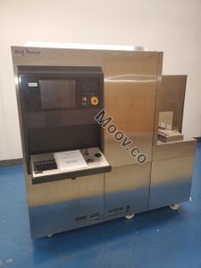
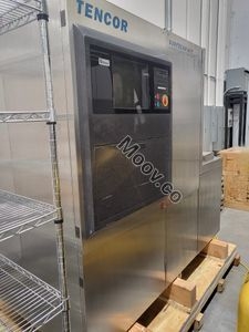
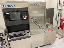
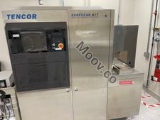
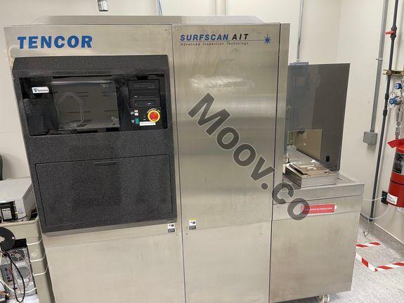
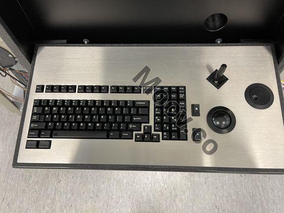
- Currently Configured for 6"/150mm & 8"/200mm Wafers - Double Darkfield Inspection Tool - SECS II/GEM Communication Interface - Low Contact Chuck (AIT I) - Multi Channel Collection Optics System with Independent Programmable Spatial Filters - Pentium CPU with Windows NT Installed - Wafer Transfer Area Housing Cover - Wafer Handling Module - High Voltage Electronics - Front and Rear EMO’s with Covers - Flat Panel Display for AIT - Fold Down Keyboard Tray with Built In Mouse - X/Y Drive/Controller Chassis and Motion Controller Card - Blower Box (exhaust hoses not included) - Operations Manual and DocumentationOEMモデルの説明
The AIT In-line Defect Inspection System is a high-throughput system that uses proprietary double-darkfield (DDF) laser scanning technology to detect defects, microscratches, and particulate contamination on wafers. It can inspect up to 30 wafers per hour at maximum sensitivity and has a low cost-per-inspection, making it economically feasible to perform in-line process monitoring at more process levels. The system achieves exceptional defect sensitivity through innovations such as a reduced laser spot size and a unique double-darkfield laser scattering design.ドキュメント
ドキュメントなし

同様のリスト
すべて表示


KLA
AIT I
カテゴリ
Defect Inspection
最終検証: 60日以上前

主なアイテムの詳細
状態:
Used
稼働ステータス:
不明
製品ID:
15509
ウェーハサイズ:
6"/150mm, 8"/200mm
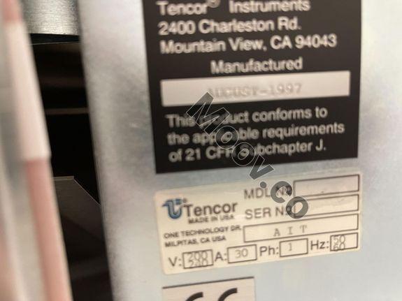
ヴィンテージ:
1997
Logistics Support
Available
Transaction Insured by Moov
Available
Refurbishment Services
Available
説明
説明なし構成
- Currently Configured for 6"/150mm & 8"/200mm Wafers - Double Darkfield Inspection Tool - SECS II/GEM Communication Interface - Low Contact Chuck (AIT I) - Multi Channel Collection Optics System with Independent Programmable Spatial Filters - Pentium CPU with Windows NT Installed - Wafer Transfer Area Housing Cover - Wafer Handling Module - High Voltage Electronics - Front and Rear EMO’s with Covers - Flat Panel Display for AIT - Fold Down Keyboard Tray with Built In Mouse - X/Y Drive/Controller Chassis and Motion Controller Card - Blower Box (exhaust hoses not included) - Operations Manual and DocumentationOEMモデルの説明
The AIT In-line Defect Inspection System is a high-throughput system that uses proprietary double-darkfield (DDF) laser scanning technology to detect defects, microscratches, and particulate contamination on wafers. It can inspect up to 30 wafers per hour at maximum sensitivity and has a low cost-per-inspection, making it economically feasible to perform in-line process monitoring at more process levels. The system achieves exceptional defect sensitivity through innovations such as a reduced laser spot size and a unique double-darkfield laser scattering design.ドキュメント
ドキュメントなし