


説明
Wafer Surface Inspection System, Surfscan構成
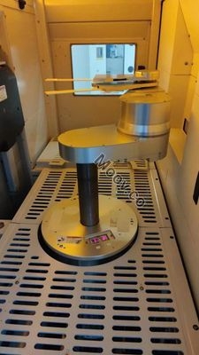
KLA Surfscan SP 2 Particle Defect System - HDD and Software Included - 4 Color Light Tower (RYGB) - Ion Shower for Phoenix Dual 12" PSL 0.04 µm (40nm) 12" PSL 0.06 µm (60nm) 12" PSL 0.083 µm (83nm) 12" PSL 0.102 µm (102nm) 12" PSL 0.155 µm (155nm) - 300 mm XY Calibration Wafer - Dryer for COE - Optimized sensitivity and throughput - < 37 nm defect sensitivity on polished bare silicon - Enables qualification of current and next-generation substrates, SOI, strained SOI and strained Si - Qualification and monitoring of process tools, at the 90, 65 and 45 nm technology nodes Assists in process troubleshooting and development Includes the following components: - UV laser - Defect map and histogram with zoom - iMicroView measurement capability - SURFimage - Real-Time Defect Classification (RTDC) - Microsoft Windows XP Operating System Features the following inspection modes: - Standard Throughput Inspection Mode - High Sensitivity Inspection Mode Advanced Illumination Optics supporting the following mode(s): - Oblique Illumination - IDM - High Sensitivity Inspect Mode - Std Throughput Inspect mode - 20 Degree - 40 Degree - Equipped with Powder Coat Painted Panels Includes 300mm Phoenix Dual FIMS Vacuum Wafer Handler (PP) Ballroom Configuration (Standard) Configured for ELB (ASIA) Power Inlet Includes the following enable licenses: - Optical Filter - Enhanced XY Coordinates - 2 mm Edge Exclusion - Standard Classification Package - LPD-N Classification - LPD-ES Classification - Grading and Sorting - Haze - Haze Analysis and Normalization - Haze Line Classification - Rough Films - NGS Desktop Software Package - Host ID will be required during software installation 2011 VintageOEMモデルの説明
The Surfscan SP2 is an unpatterned wafer surface inspection tool that uses UV laser technology, darkfield optics, and advanced algorithms to detect defects as small as 30nm. It provides high sensitivity detection on engineered substrates and has a significant throughput increase over the prior-generation tool. It offers a single tool solution for three technology nodes and has comprehensive wafer surface inspection capabilities. It also enables faster root-cause analysis with improved coordinate accuracy and real-time defect classification capability.ドキュメント

検証済み
カテゴリ
Defect Inspection
最終検証: 60日以上前
主なアイテムの詳細
状態:
Used
稼働ステータス:
不明
製品ID:
136585
ウェーハサイズ:
不明
ヴィンテージ:
2011
Logistics Support
Available
Transaction Insured by Moov
Available
Refurbishment Services
Available
同様のリスト
すべて表示


KLA
SURFSCAN SP2
カテゴリ
Defect Inspection
最終検証: 60日以上前


主なアイテムの詳細
状態:
Used
稼働ステータス:
不明
製品ID:
136585
ウェーハサイズ:
不明
ヴィンテージ:
2011
Logistics Support
Available
Transaction Insured by Moov
Available
Refurbishment Services
Available