


説明
HDD not included構成
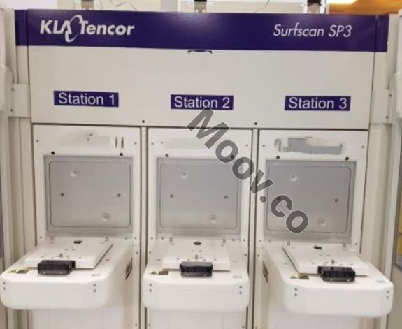
KLA Surfscan SP3 Defect and Surface Quality Inspection Systems – UDL/UDK KLA SP3 Main Components - •Integrated Console •Bare Wafer Inspection Station •Equipment Front End Module (EFEM) •3 Port Wafer Loading Unit Description of Inspection System - •Un-patterned wafer inspection platform to incorporate deep-ultraviolet (DUV) illumination. Deep Ultraviolet(DUV) source •DUV-specific apertures to enable defect capture on un-patterned thin films •High speed stage and advanced imaging computer for enhanced productivity •Full-wafer high-resolution haze maps Defect Detection and Classification Capabilities •Designed to capture a broad range of challenging defects for 32nm/22nm process nodes •High-productivity rapid automated defect classification •Coordinate accuracy to enable rapid defect re-detection and review •Integrated, high resolution (~100 mega-pixel), full-wafer SURF monitor™ haze maps, providing automated capture of ultra-fine slip lines and scratches or maps of surface roughness, grain size and other process parameters •Surfscan SP3 system feature dramatic advances in sensitivity and throughput over their industry-benchmark predecessor, the Surfscan SP2XP •Inspection Module for the back side of wafers for defects that might deform the wafer shape.OEMモデルの説明
The Surfscan® SP3 is an unpatterned wafer inspection tool available in 450mm, 300mm, and 300mm/450mm bridge tool configurations. It uses deep ultra-violet (DUV) sensitivity and has a throughput up to three times that of its predecessor. It can detect critical defects and surface quality issues for IC, OEM, and substrate manufacturing at the 2Xnm design node. The tool also includes an integrated SURFmonitor module that characterizes and measures surface quality. It has flexible configurations and a reliable, extendible architecture. It is used for qualification and monitoring of process tools for the 2Xnm design node within the IC fab, as well as serving as a lithography process tool monitor. The Surfscan SP3 can also be used for incoming wafer qualification, inline process control, final wafer qualification, process tool qualification, and as a process uniformity monitor.ドキュメント

検証済み
カテゴリ
Defect Inspection
最終検証: 60日以上前
主なアイテムの詳細
状態:
Used
稼働ステータス:
Deinstalled
製品ID:
137249
ウェーハサイズ:
不明
ヴィンテージ:
2015
Logistics Support
Available
Transaction Insured by Moov
Available
Refurbishment Services
Available
同様のリスト
すべて表示


KLA
SURFSCAN SP3
カテゴリ
Defect Inspection
最終検証: 60日以上前


主なアイテムの詳細
状態:
Used
稼働ステータス:
Deinstalled
製品ID:
137249
ウェーハサイズ:
不明
ヴィンテージ:
2015
Logistics Support
Available
Transaction Insured by Moov
Available
Refurbishment Services
Available