


説明
説明なし構成
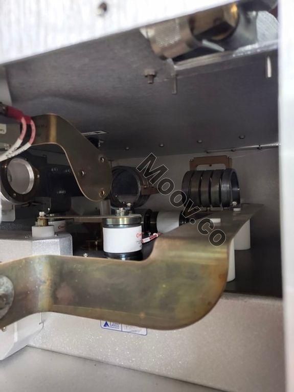
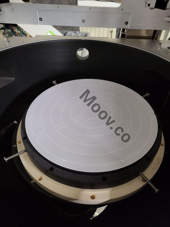
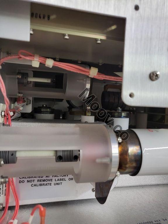
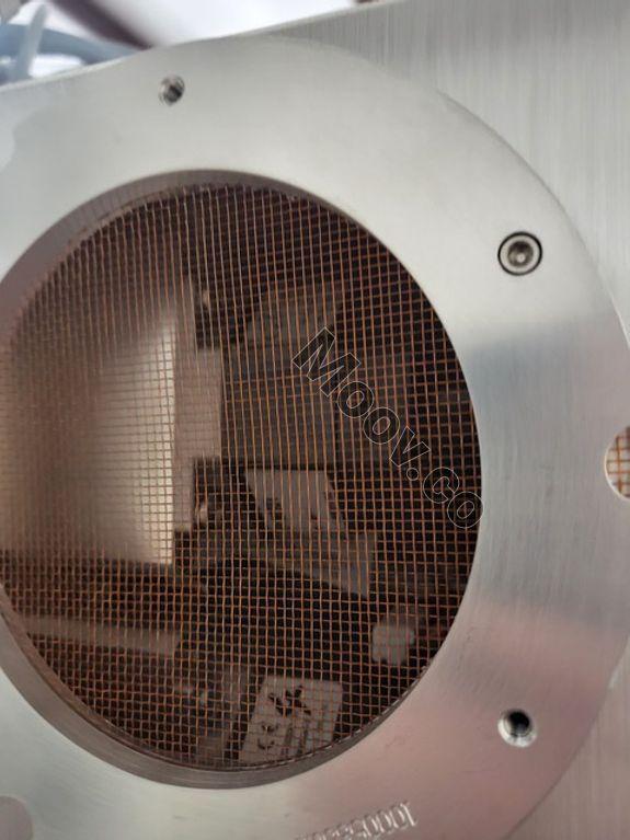
LAM Kiyo 45 Chamber Has missing partsOEMモデルの説明
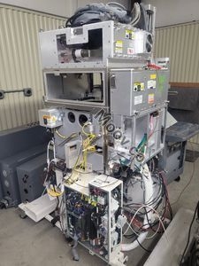
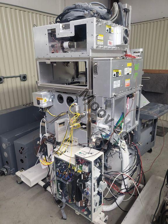
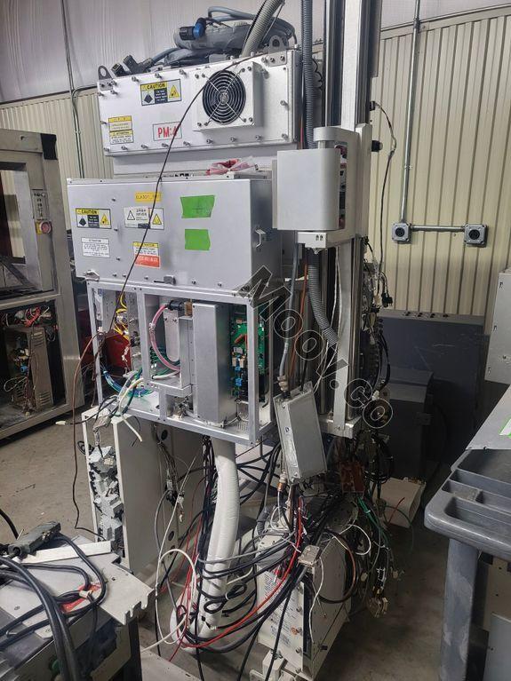
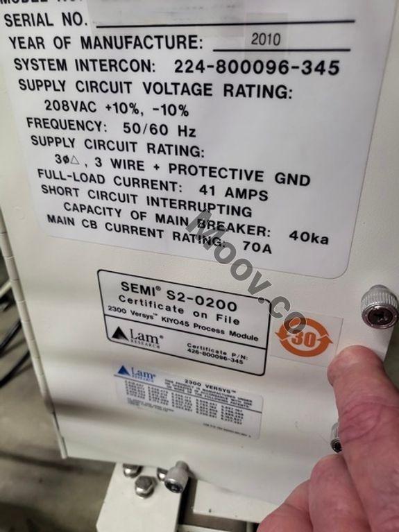
The 2300 Versys Kiyo45 is a Reactive Ion Etch (RIE) system from Lam Research, part of the Kiyo Product Family. It is used to shape the electrically active materials of a semiconductor device with high precision and consistency. The Kiyo product family is known for its high-performance capabilities and productivity. The Versys Kiyo45 is used for various applications, including shallow trench isolation, source/drain engineering, high-k/metal gate, FinFET and tri-gate, and multi-patterning. It enables processing at sub-65 nm technology nodes.ドキュメント
ドキュメントなし

カテゴリ
Dry / Plasma Etch
最終検証: 60日以上前
主なアイテムの詳細
状態:
Parts Tool
稼働ステータス:
Deinstalled
製品ID:
97779
ウェーハサイズ:
不明
ヴィンテージ:
不明
Logistics Support
Available
Transaction Insured by Moov
Available
Refurbishment Services
Available

LAM RESEARCH CORPORATION
2300 VERSYS KIYO45
カテゴリ
Dry / Plasma Etch
最終検証: 60日以上前

主なアイテムの詳細
状態:
Parts Tool
稼働ステータス:
Deinstalled
製品ID:
97779
ウェーハサイズ:
不明
ヴィンテージ:
不明
Logistics Support
Available
Transaction Insured by Moov
Available
Refurbishment Services
Available
説明
説明なし構成
LAM Kiyo 45 Chamber Has missing partsOEMモデルの説明
The 2300 Versys Kiyo45 is a Reactive Ion Etch (RIE) system from Lam Research, part of the Kiyo Product Family. It is used to shape the electrically active materials of a semiconductor device with high precision and consistency. The Kiyo product family is known for its high-performance capabilities and productivity. The Versys Kiyo45 is used for various applications, including shallow trench isolation, source/drain engineering, high-k/metal gate, FinFET and tri-gate, and multi-patterning. It enables processing at sub-65 nm technology nodes.ドキュメント
ドキュメントなし