


説明
説明なし構成
構成なしOEMモデルの説明
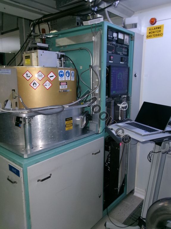
The Novellus Concept-One is a PECVD tool that uses plasma-enhanced chemical vapor deposition to deposit various dielectric films on silicon wafers. It can deposit oxide, nitride, oxynitride, PSG and TEOS oxide films. The Concept1 is also a PECVD tool that deposits dielectric films on 6" wafers. It is capable of depositing thick films in excess of 1 um and allows CMOS compatible metals, making it suitable for backend processes. The system deposits on multiple wafers in parallel in a batch-type reactor.ドキュメント
ドキュメントなし

カテゴリ
PECVD
最終検証: 60日以上前
主なアイテムの詳細
状態:
Used
稼働ステータス:
不明
製品ID:
145124
ウェーハサイズ:
6"/150mm
ヴィンテージ:
1995
Logistics Support
Available
Transaction Insured by Moov
Available
Refurbishment Services
Available
同様のリスト
すべて表示


LAM RESEARCH / NOVELLUS
CONCEPT ONE "C1"
カテゴリ
PECVD
最終検証: 60日以上前


主なアイテムの詳細
状態:
Used
稼働ステータス:
不明
製品ID:
145124
ウェーハサイズ:
6"/150mm
ヴィンテージ:
1995
Logistics Support
Available
Transaction Insured by Moov
Available
Refurbishment Services
Available
説明
説明なし構成
構成なしOEMモデルの説明
The Novellus Concept-One is a PECVD tool that uses plasma-enhanced chemical vapor deposition to deposit various dielectric films on silicon wafers. It can deposit oxide, nitride, oxynitride, PSG and TEOS oxide films. The Concept1 is also a PECVD tool that deposits dielectric films on 6" wafers. It is capable of depositing thick films in excess of 1 um and allows CMOS compatible metals, making it suitable for backend processes. The system deposits on multiple wafers in parallel in a batch-type reactor.ドキュメント
ドキュメントなし