


説明
説明なし構成
構成なしOEMモデルの説明
The Eclipse Mark IV is the latest generation PVD tool from the highly successful Eclipse family. It offers the lowest Cost-of-Ownership through high throughput, a small footprint, and high reliability with exceptional process performance. The system achieves high throughput in a high vacuum environment through the use of serial wafer handling, resulting in 80% fewer wafer transfers than a traditional cluster tool. The Eclipse Mark IV has a footprint of 44 square feet and can be configured for etch or deposition, providing full capability for today’s contact, barrier, interconnect, resistor, and packaging films for Silicon, GaAs and CCD substrates. Wafer temperature is regulated by backplane heaters and the chambers have world class vacuum leak rates and base pressures.ドキュメント
ドキュメントなし
TEL / MRC
ECLIPSE MARK IV

検証済み
カテゴリ
PVD / Sputtering
最終検証: 60日以上前
主なアイテムの詳細
状態:
Used
稼働ステータス:
不明
製品ID:
79339
ウェーハサイズ:
6"/150mm
ヴィンテージ:
不明
Have Additional Questions?
Logistics Support
Available
Money Back Guarantee
Available
Transaction Insured by Moov
Available
Refurbishment Services
Available
同様のリスト
すべて表示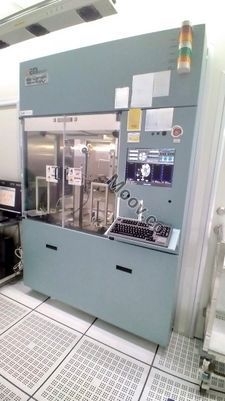


TEL / MRC
ECLIPSE MARK IV
カテゴリ
PVD / Sputtering
最終検証: 60日以上前


主なアイテムの詳細
状態:
Used
稼働ステータス:
不明
製品ID:
79339
ウェーハサイズ:
6"/150mm
ヴィンテージ:
不明
Have Additional Questions?
Logistics Support
Available
Money Back Guarantee
Available
Transaction Insured by Moov
Available
Refurbishment Services
Available
説明
説明なし構成
構成なしOEMモデルの説明
The Eclipse Mark IV is the latest generation PVD tool from the highly successful Eclipse family. It offers the lowest Cost-of-Ownership through high throughput, a small footprint, and high reliability with exceptional process performance. The system achieves high throughput in a high vacuum environment through the use of serial wafer handling, resulting in 80% fewer wafer transfers than a traditional cluster tool. The Eclipse Mark IV has a footprint of 44 square feet and can be configured for etch or deposition, providing full capability for today’s contact, barrier, interconnect, resistor, and packaging films for Silicon, GaAs and CCD substrates. Wafer temperature is regulated by backplane heaters and the chambers have world class vacuum leak rates and base pressures.ドキュメント
ドキュメントなし