


説明
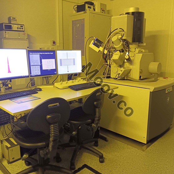
FIB Equipped with 100mm² EDS構成
Electron Source: Schottky thermal field emitter Accelerating Voltage Range: 350 V – 30 kV (Landing voltage in beam deceleration mode: 20 V – 30 kV) Probe Current Range: 0.7 pA – 22 nA Resolution: Best Working Distance: 0.8 nm @ 30 kV (STEM) 0.9 nm @ 15 kV ; 1.4 nm @ 1 kV Beam Coincidence Point: 0.9 – 1.0 nm @ 15 kV 1.6 nm @ 5 kV ; 2.5 nm @ 1 kV Bruker EDS: 100mm2 Detector (brand new detector installed in 2024)Gas Injection System (GIS): Pt and XeF2 (includes 2 gas injection needles/canisters)Automatic 3D Slice and 3DView: Integrated fully automatic 3D reconstruction software KLEINDIEK NANOTECHNIK MM3A-EM Manipulator: (Non-OEM / third-party manipulator)OEMモデルの説明
The Helios NanoLab 600 is a Dual Beam FIB/SEM (Focused Ion Beam/Scanning Electron Microscope) that is designed for high-end imaging during failure analysis. It features an extreme high-resolution column, a fine-probe ion source, and a 150 x 150 mm, five-axis, XY piezo stage. This makes it a smart investment for failure-analysis labs that require versatile sample handling, from packaged parts to eight-inch wafers. The Helios NanoLab 600 is particularly useful for cross-sectioning samples and delivers three-dimensional imaging, allowing you to quickly and efficiently locate and view device features from different angles. Additionally, patented beam chemistries can be used to highlight interface layers for imaging in the system, providing you with the most accurate data possible without additional preparation steps outside the system.ドキュメント
ドキュメントなし

カテゴリ
SEM / FIB
最終検証: 23日前
主なアイテムの詳細
状態:
Used
稼働ステータス:
不明
製品ID:
153199
ウェーハサイズ:
不明
ヴィンテージ:
2010
Logistics Support
Available
Transaction Insured by Moov
Available
Refurbishment Services
Available
同様のリスト
すべて表示

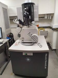


THERMOFISHER SCIENTIFIC / FEI / PHILIPS
HELIOS NANOLAB 600
カテゴリ
SEM / FIB
最終検証: 23日前


主なアイテムの詳細
状態:
Used
稼働ステータス:
不明
製品ID:
153199
ウェーハサイズ:
不明
ヴィンテージ:
2010
Logistics Support
Available
Transaction Insured by Moov
Available
Refurbishment Services
Available
説明
FIB Equipped with 100mm² EDS構成
Electron Source: Schottky thermal field emitter Accelerating Voltage Range: 350 V – 30 kV (Landing voltage in beam deceleration mode: 20 V – 30 kV) Probe Current Range: 0.7 pA – 22 nA Resolution: Best Working Distance: 0.8 nm @ 30 kV (STEM) 0.9 nm @ 15 kV ; 1.4 nm @ 1 kV Beam Coincidence Point: 0.9 – 1.0 nm @ 15 kV 1.6 nm @ 5 kV ; 2.5 nm @ 1 kV Bruker EDS: 100mm2 Detector (brand new detector installed in 2024)Gas Injection System (GIS): Pt and XeF2 (includes 2 gas injection needles/canisters)Automatic 3D Slice and 3DView: Integrated fully automatic 3D reconstruction software KLEINDIEK NANOTECHNIK MM3A-EM Manipulator: (Non-OEM / third-party manipulator)OEMモデルの説明
The Helios NanoLab 600 is a Dual Beam FIB/SEM (Focused Ion Beam/Scanning Electron Microscope) that is designed for high-end imaging during failure analysis. It features an extreme high-resolution column, a fine-probe ion source, and a 150 x 150 mm, five-axis, XY piezo stage. This makes it a smart investment for failure-analysis labs that require versatile sample handling, from packaged parts to eight-inch wafers. The Helios NanoLab 600 is particularly useful for cross-sectioning samples and delivers three-dimensional imaging, allowing you to quickly and efficiently locate and view device features from different angles. Additionally, patented beam chemistries can be used to highlight interface layers for imaging in the system, providing you with the most accurate data possible without additional preparation steps outside the system.ドキュメント
ドキュメントなし