We value your privacy
We and our selected partners use cookies to enhance your browsing experience, serve personalized content, and analyze our traffic. By clicking "Accept All", you consent to our use of cookies. 続きを読む


ドキュメントなし
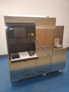
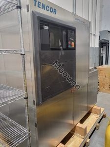
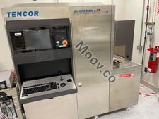
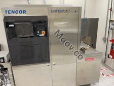
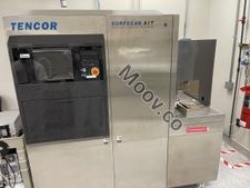
KLA
Used
不明
56610
不明
不明
ドキュメントなし