


説明
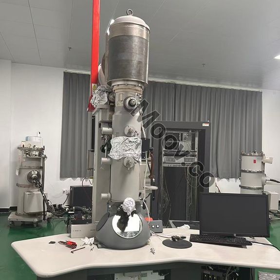
A 200kV field emission transmission electron microscope that combines high-resolution imaging with powerful chemical composition analysis capabilities. Description 1. Main Instrument (FEI Tecnai T20)Transmission Electron Microscope Main Unit: FEI Tecnai T20• Schottky Field Emission Gun (FEG)• System Column• Workstation + LCD Monitor• Control Panels x 2• 200kV High Voltage Box• Power control cabinet 2. Bottom-Mount Digital Camera: Gatan 894 Camera (4M) 1 3. Align Genie (Alignment): Microscope Alignment File (One free-of-charge Alignments at 200 kV) 1 4. Cooler / Compressor: Air Compressor (Compressor) 1 5 Cooler / Compressor : Water Chiller (Cooler) 1 6 Vacuum System: Mechanical Pump, Molecular Pump, Ion Pump 1 7 Software and Control Systems: Operating System: Windows-based operating system 1 8 Software and Control Systems: Control Software: FEI TUI software platform, used to control all microscope functions, lenses, alignments, cameras, and accessories構成
Accelerating Voltage: Maximum 200kV, supporting multi-gear adjustment at 100kV/120kV/160kV/200kV to accommodate different sample thicknesses and imaging needs. Electron Gun Type: Equipped with a $\text{LaB}_6$ (Lanthanum Hexaboride) electron gun featuring high brightness ($>1\times10^6\text{ A/cm}^2\cdot\text{sr}$) and low emission half-angle characteristics, ensuring electron beam stability and imaging resolution. Resolution • Point Resolution: $<0.25\text{ nm}$ (at 200kV, meeting atomic-level detail observation needs) • Line Resolution: $<0.102\text{ nm}$ (under high-resolution mode, clearly revealing crystal lattice structures) Magnification: Covers a broad magnification range from $25\times$ to $1,000,000\times$, seamlessly switching from low-magnification morphology observation to high-magnification structural analysis. Sample Stage: Standard double-tilt sample stage (tilt angles: $\pm 60^\circ$ ($\alpha$-axis), $\pm 30^\circ$ ($\beta$-axis)), supporting high-precision positioning and tilting, compatible with standard 3mm TEM grid samples. Imaging Modes: Supports Bright-Field (BF), Dark-Field (DF), and High-Resolution Transmission Electron Microscopy (HRTEM) imaging to meet diverse microstructural characterization needs.OEMモデルの説明
提供なしドキュメント
ドキュメントなし

カテゴリ
TEM
最終検証: 30日以上前
主なアイテムの詳細
状態:
Used
稼働ステータス:
不明
製品ID:
151894
ウェーハサイズ:
不明
ヴィンテージ:
2007
Logistics Support
Available
Transaction Insured by Moov
Available
Refurbishment Services
Available
同様のリスト
すべて表示


THERMOFISHER SCIENTIFIC / FEI / PHILIPS
Tecnai T20
カテゴリ
TEM
最終検証: 30日以上前


主なアイテムの詳細
状態:
Used
稼働ステータス:
不明
製品ID:
151894
ウェーハサイズ:
不明
ヴィンテージ:
2007
Logistics Support
Available
Transaction Insured by Moov
Available
Refurbishment Services
Available
説明
A 200kV field emission transmission electron microscope that combines high-resolution imaging with powerful chemical composition analysis capabilities. Description 1. Main Instrument (FEI Tecnai T20)Transmission Electron Microscope Main Unit: FEI Tecnai T20• Schottky Field Emission Gun (FEG)• System Column• Workstation + LCD Monitor• Control Panels x 2• 200kV High Voltage Box• Power control cabinet 2. Bottom-Mount Digital Camera: Gatan 894 Camera (4M) 1 3. Align Genie (Alignment): Microscope Alignment File (One free-of-charge Alignments at 200 kV) 1 4. Cooler / Compressor: Air Compressor (Compressor) 1 5 Cooler / Compressor : Water Chiller (Cooler) 1 6 Vacuum System: Mechanical Pump, Molecular Pump, Ion Pump 1 7 Software and Control Systems: Operating System: Windows-based operating system 1 8 Software and Control Systems: Control Software: FEI TUI software platform, used to control all microscope functions, lenses, alignments, cameras, and accessories構成
Accelerating Voltage: Maximum 200kV, supporting multi-gear adjustment at 100kV/120kV/160kV/200kV to accommodate different sample thicknesses and imaging needs. Electron Gun Type: Equipped with a $\text{LaB}_6$ (Lanthanum Hexaboride) electron gun featuring high brightness ($>1\times10^6\text{ A/cm}^2\cdot\text{sr}$) and low emission half-angle characteristics, ensuring electron beam stability and imaging resolution. Resolution • Point Resolution: $<0.25\text{ nm}$ (at 200kV, meeting atomic-level detail observation needs) • Line Resolution: $<0.102\text{ nm}$ (under high-resolution mode, clearly revealing crystal lattice structures) Magnification: Covers a broad magnification range from $25\times$ to $1,000,000\times$, seamlessly switching from low-magnification morphology observation to high-magnification structural analysis. Sample Stage: Standard double-tilt sample stage (tilt angles: $\pm 60^\circ$ ($\alpha$-axis), $\pm 30^\circ$ ($\beta$-axis)), supporting high-precision positioning and tilting, compatible with standard 3mm TEM grid samples. Imaging Modes: Supports Bright-Field (BF), Dark-Field (DF), and High-Resolution Transmission Electron Microscopy (HRTEM) imaging to meet diverse microstructural characterization needs.OEMモデルの説明
提供なしドキュメント
ドキュメントなし