


説明
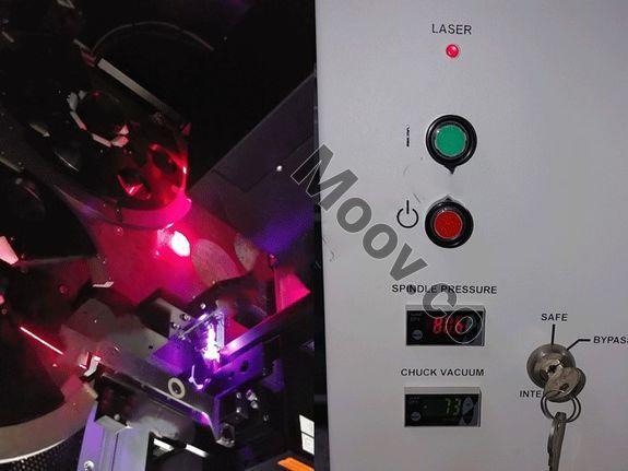
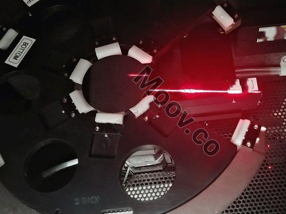
KLA-Tencor Candela 8620 KLA-Tencor Candela 8620 Optical Surface Analyzer (OSA) is a laser-based inspection system for semiconductor and optoelectronic wafers. It is fully automated with integrated wafer handling for cassette-to-cassette operation. The Candela defect detection system simultaneously measures surface reflectivity and topography for automatic defect detection and classification. The defect detection system's inspection technology combines scatterometry, ellipsometry, reflectometry, and topographical analysis to non-destructively inspect wafer surfaces for defects, and film thickness uniformity, of opaque substrates, epi layers, and transparent film coatings (SiC, GaN, sapphire).構成
- Cassette Handling - Laser: Oblique(50mW, 405nm), Normal(85mW, 660nm) - Spot size: 5㎛ x 4㎛. - Handler: Mapping, Wafer centering on chuck and FFM: OK, Wafer loading/unloading: OK - Particle detection: smaller than 0.08㎛ on silicon substrate. - Scratch: 0.1㎛ wide, 1~2nm deep. - Pits and Bumps: 20㎛ diameter, 50Å;; deep. - Stains: 20㎛ diameter, 10Å;; thick. - can be used for both epi and bare substrate. - can be used for Si, GaAs, Al2O3,SiC substrate. - Substrage thickness: 350㎛ ~ 1,300㎛. - Air Balance system ULPA and HEPA air filter(replaced new one). - Input Power 230V 6A 50/60Hz - Input Air: CDA 90 PSIOEMモデルの説明
The Candela 8620 is an automated defect inspection system for LED substrates and epitaxy wafers. It provides enhanced quality control for materials such as gallium nitride, sapphire, and silicon carbide. Its proprietary optical design and detection technology can detect sub-micron defects that are not consistently identified by current inspection methods. This enables a production line monitor for yield-limiting defects, improving MOCVD reactor uptime and yield. The system can detect defects such as micro-scratches, micro-cracks, missing bumps, resist voids, hexagonal pits, and epi cracks, which can impact device performance, yield, and reliability.ドキュメント
ドキュメントなし

検証済み
カテゴリ
Defect Inspection
最終検証: 60日以上前
主なアイテムの詳細
状態:
Refurbished
稼働ステータス:
不明
製品ID:
65985
ウェーハサイズ:
8"/200mm
ヴィンテージ:
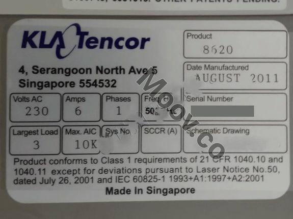
2011
Logistics Support
Available
Transaction Insured by Moov
Available
Refurbishment Services
Available
同様のリスト
すべて表示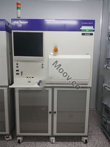


KLA
CANDELA 8620
カテゴリ
Defect Inspection
最終検証: 60日以上前

主なアイテムの詳細
状態:
Refurbished
稼働ステータス:
不明
製品ID:
65985
ウェーハサイズ:
8"/200mm
ヴィンテージ:
2011
Logistics Support
Available
Transaction Insured by Moov
Available
Refurbishment Services
Available
説明
KLA-Tencor Candela 8620 KLA-Tencor Candela 8620 Optical Surface Analyzer (OSA) is a laser-based inspection system for semiconductor and optoelectronic wafers. It is fully automated with integrated wafer handling for cassette-to-cassette operation. The Candela defect detection system simultaneously measures surface reflectivity and topography for automatic defect detection and classification. The defect detection system's inspection technology combines scatterometry, ellipsometry, reflectometry, and topographical analysis to non-destructively inspect wafer surfaces for defects, and film thickness uniformity, of opaque substrates, epi layers, and transparent film coatings (SiC, GaN, sapphire).構成
- Cassette Handling - Laser: Oblique(50mW, 405nm), Normal(85mW, 660nm) - Spot size: 5㎛ x 4㎛. - Handler: Mapping, Wafer centering on chuck and FFM: OK, Wafer loading/unloading: OK - Particle detection: smaller than 0.08㎛ on silicon substrate. - Scratch: 0.1㎛ wide, 1~2nm deep. - Pits and Bumps: 20㎛ diameter, 50Å;; deep. - Stains: 20㎛ diameter, 10Å;; thick. - can be used for both epi and bare substrate. - can be used for Si, GaAs, Al2O3,SiC substrate. - Substrage thickness: 350㎛ ~ 1,300㎛. - Air Balance system ULPA and HEPA air filter(replaced new one). - Input Power 230V 6A 50/60Hz - Input Air: CDA 90 PSIOEMモデルの説明
The Candela 8620 is an automated defect inspection system for LED substrates and epitaxy wafers. It provides enhanced quality control for materials such as gallium nitride, sapphire, and silicon carbide. Its proprietary optical design and detection technology can detect sub-micron defects that are not consistently identified by current inspection methods. This enables a production line monitor for yield-limiting defects, improving MOCVD reactor uptime and yield. The system can detect defects such as micro-scratches, micro-cracks, missing bumps, resist voids, hexagonal pits, and epi cracks, which can impact device performance, yield, and reliability.ドキュメント
ドキュメントなし