


説明
説明なし構成
. Automatic robotic wafer handling . Single open-cassette wafer loading station Non-contact CV/IV Measurement System . Measurement of dielectric and interface properties on monitor wafer - Dielectric Capacitance (CD) and Thickness (EOT) - Dielectric Leakage Current (I-V) - Flatband Voltage (Vfb) - Interface Trap Density (Dit) - Interface Trapped Charge (Qit) - Semiconductor Surface Barrier (Vsb) - Oxide Total Charge (Qtot) - Mobile Ionic Charge (Qm), among others . Suitable for measurement on: - Semiconductor wafers (e.g. Si, SiGe, InGaAs, SiC, GaN) with high-k and low-k dielectric films (e.g. SiO2, SiNx, Al2O3, HfO2 ;..)OEMモデルの説明
The SEMILAB FAAST 230 is a non-contact, fast in-line monitoring system designed to detect heavy metal contamination, including sub 108 atoms/cm-3 Fe detection, in a medium to high-volume manufacturing environment. It features automated wafer handling, with options for SMIF/FOUP Loadport/Versaport, and can perform full wafer FAST mapping of diffusion length, Iron, and other recombination centers. The system is configurable for 100 mm to 300 mm wafers and is compatible with other Semilab SDI FAaST tool measurement technologies. Additional options include a minienvironment, wafer edge-grip handling, wafer flipper for automatic backsurface measurement, and more.ドキュメント
ドキュメントなし

同様のリスト
すべて表示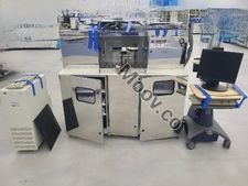


SEMILAB
FAAST 230
カテゴリ
Defect Inspection
最終検証: 60日以上前


主なアイテムの詳細
状態:
Used
稼働ステータス:
不明
製品ID:
102007
ウェーハサイズ:
8"/200mm
ヴィンテージ:
2000
Logistics Support
Available
Transaction Insured by Moov
Available
Refurbishment Services
Available
説明
説明なし構成
. Automatic robotic wafer handling . Single open-cassette wafer loading station Non-contact CV/IV Measurement System . Measurement of dielectric and interface properties on monitor wafer - Dielectric Capacitance (CD) and Thickness (EOT) - Dielectric Leakage Current (I-V) - Flatband Voltage (Vfb) - Interface Trap Density (Dit) - Interface Trapped Charge (Qit) - Semiconductor Surface Barrier (Vsb) - Oxide Total Charge (Qtot) - Mobile Ionic Charge (Qm), among others . Suitable for measurement on: - Semiconductor wafers (e.g. Si, SiGe, InGaAs, SiC, GaN) with high-k and low-k dielectric films (e.g. SiO2, SiNx, Al2O3, HfO2 ;..)OEMモデルの説明
The SEMILAB FAAST 230 is a non-contact, fast in-line monitoring system designed to detect heavy metal contamination, including sub 108 atoms/cm-3 Fe detection, in a medium to high-volume manufacturing environment. It features automated wafer handling, with options for SMIF/FOUP Loadport/Versaport, and can perform full wafer FAST mapping of diffusion length, Iron, and other recombination centers. The system is configurable for 100 mm to 300 mm wafers and is compatible with other Semilab SDI FAaST tool measurement technologies. Additional options include a minienvironment, wafer edge-grip handling, wafer flipper for automatic backsurface measurement, and more.ドキュメント
ドキュメントなし