


説明
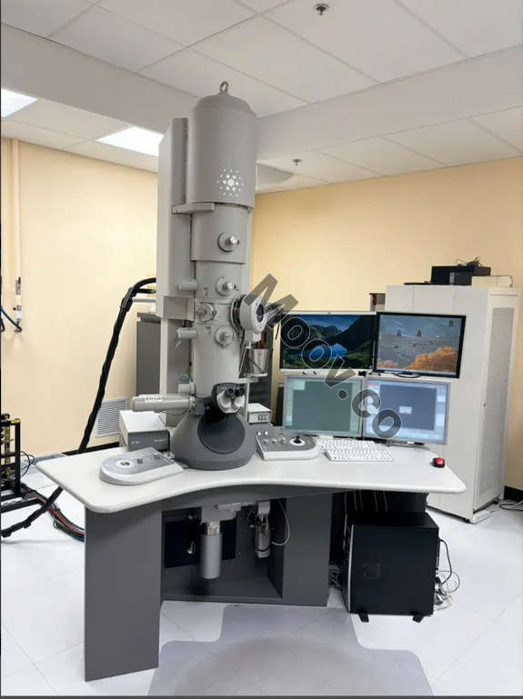
FEI Tecnai G2 F20 + EELS + EDS + GIF構成
Thermo Fisher Scientific / FEI Tecnai G2 F20 X-Twin transmission electron microscope. Schottky FEG TEM optimized for high-resolution imaging, analytical TEM, EFTEM, STEM, and spectroscopy in materials science and nanotechnology. ** BEAM ** – Field emission gun (FEG) – Acceleration voltage range: “80 to 200 kV” – FEG probe current: 0.923 nA – Spot drift: 0.424 nm/min ** RESOLUTION ** – TEM point resolution: < 0.26 nm – TEM line resolution: 0.102 nm – Information limit: < 0.14 nm – HRSTEM resolution: 0.192 nm – STEM probe size: "sub-nanometer" ** DETECTORS ** – On-axis bright field / dark field detector – Oxford X-Max 250 SDD EDS – EFTEM EELS module – CCD camera ORIUS SC1000 (model 832). – Energy resolution (GIF): 0.8 eV ** STAGE ** – X-Twin high-stability goniometer – Axes: "X, Y, Z, alpha, beta" – Maximum tilt: "±70 degrees (holder dependent)" – Specimen drift: < 0.5 nm/minOEMモデルの説明
提供なしドキュメント
ドキュメントなし


TECNAI
F20
カテゴリ
TEM
最終検証: 30日以上前


主なアイテムの詳細
状態:
Used
稼働ステータス:
不明
製品ID:
147195
ウェーハサイズ:
不明
ヴィンテージ:
2012
Logistics Support
Available
Transaction Insured by Moov
Available
Refurbishment Services
Available
説明
FEI Tecnai G2 F20 + EELS + EDS + GIF構成
Thermo Fisher Scientific / FEI Tecnai G2 F20 X-Twin transmission electron microscope. Schottky FEG TEM optimized for high-resolution imaging, analytical TEM, EFTEM, STEM, and spectroscopy in materials science and nanotechnology. ** BEAM ** – Field emission gun (FEG) – Acceleration voltage range: “80 to 200 kV” – FEG probe current: 0.923 nA – Spot drift: 0.424 nm/min ** RESOLUTION ** – TEM point resolution: < 0.26 nm – TEM line resolution: 0.102 nm – Information limit: < 0.14 nm – HRSTEM resolution: 0.192 nm – STEM probe size: "sub-nanometer" ** DETECTORS ** – On-axis bright field / dark field detector – Oxford X-Max 250 SDD EDS – EFTEM EELS module – CCD camera ORIUS SC1000 (model 832). – Energy resolution (GIF): 0.8 eV ** STAGE ** – X-Twin high-stability goniometer – Axes: "X, Y, Z, alpha, beta" – Maximum tilt: "±70 degrees (holder dependent)" – Specimen drift: < 0.5 nm/minOEMモデルの説明
提供なしドキュメント
ドキュメントなし